
Concept of compensating for piezo influences on integrated circuitry

a technology of integrated circuitry and piezo, which is applied in the field of integrated circuitry, can solve the problems of difficult reproduction of the mechanical stress or mechanical strain present in the semiconductor material of the semiconductor substrate, the inability to adapt and mount the integrated circuitry in a package, and the inability to compensate for piezo influences on the integrated circuitry. , to achieve the effect of reducing the risk of damage to the integrated circuitry, and reducing the risk of damage to the a piezo influence of integrated circuitry, the concept of integrated circuitry, the concept of integrated circuitry, the concept of integrated circuitry, the effect of piezo influence of piezo influence of integrated circuitry the effect of piezo influence, the effect of piezo influence, the effect of piezo effect, piezo influence of piezo influence of piezo influen

Active Publication Date: 2008-05-15
INFINEON TECH AG
View PDF3 Cites 22 Cited by
  • Summary
  • Abstract
  • Description
  • Claims
  • Application Information

AI Technical Summary

Benefits of technology

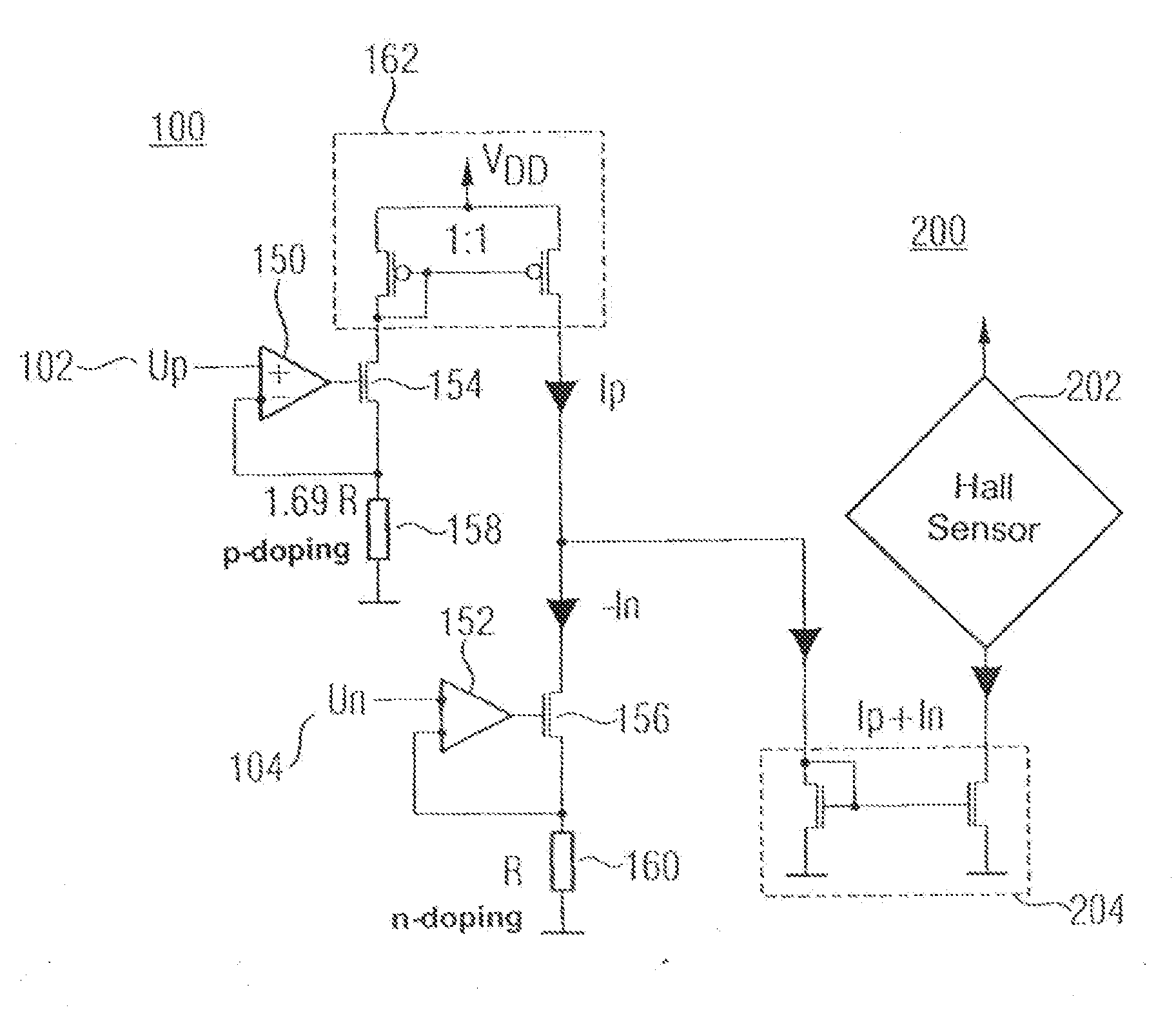
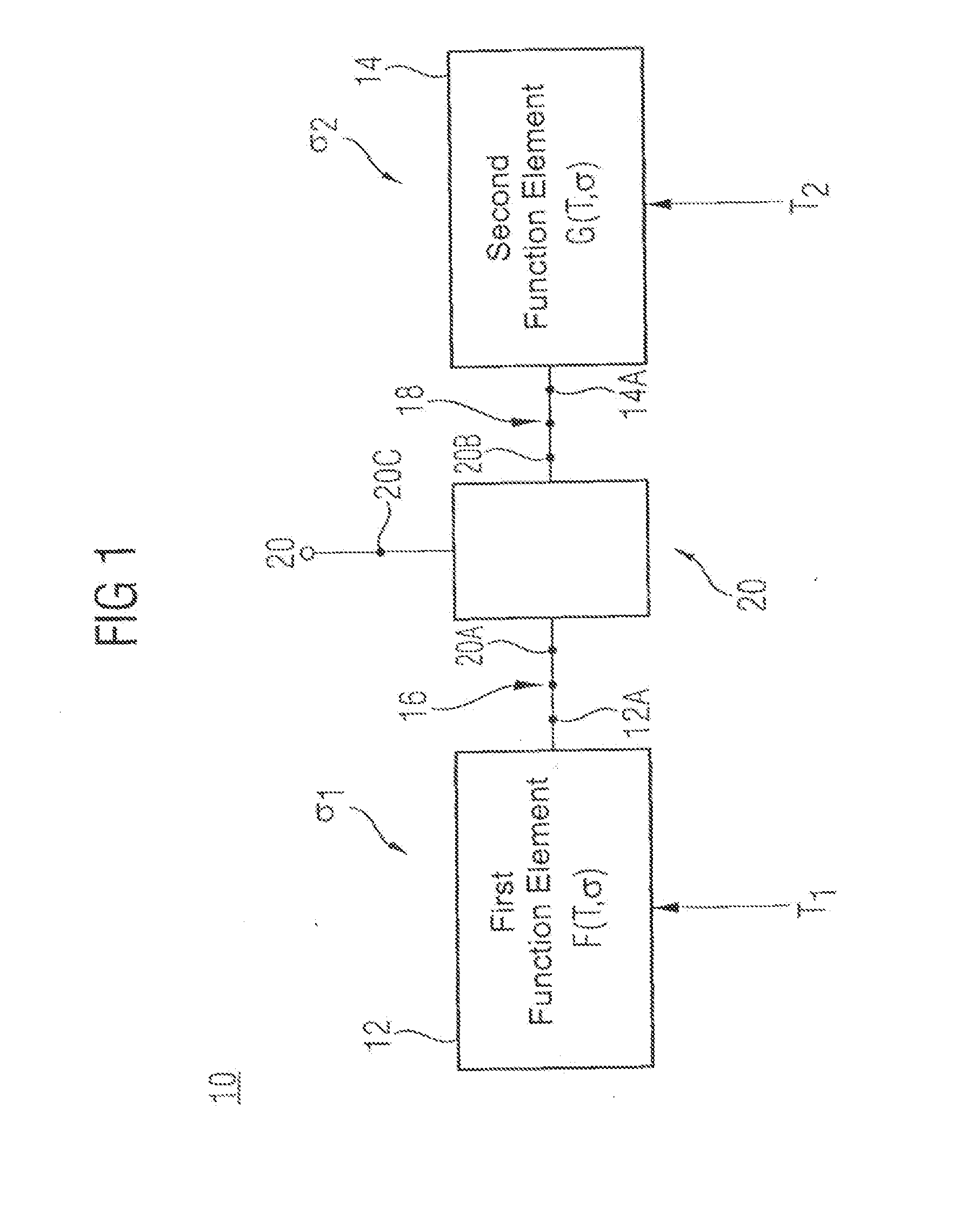
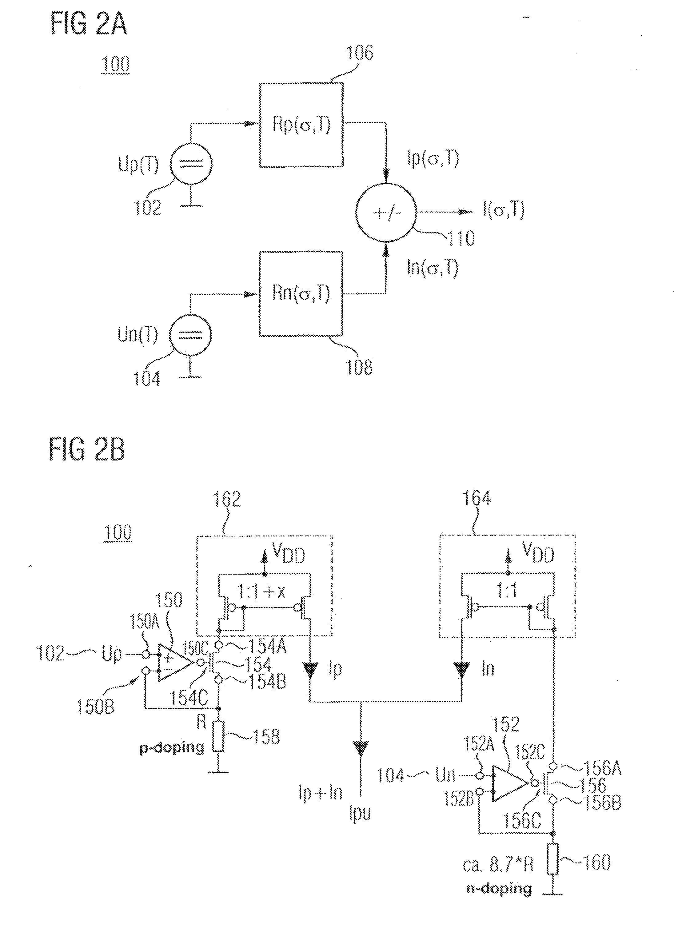
The present invention provides an improved concept for compensating for piezo influences on integrated circuitry on semiconductor chips. The invention involves combining two electronic functional elements with different functional-element parameters that exhibit a dependence on mechanical stress in the semiconductor chip. The first functional element has a first electronic functional-element parameter that depends on the mechanical stress in the chip, while the second functional element has a second electronic functional-element parameter that also depends on the mechanical stress in the chip. By combining the output signals of these two elements, a resulting output signal is obtained with a predefined dependence on the mechanical stress in the chip. The invention also provides a method for generating the output signal by integrating the two functional elements on the chip and arranging them geometrically such that the directional dependencies of the piezo influences on the two parameters are mutual and compensate for each other.

Problems solved by technology

However, one disadvantageous side effect that may be observed is that accommodating and mounting the integrated circuitry in a package exerts considerable mechanical stress on the semiconductor material, and thus on the semiconductor substrate of the integrated circuitry.
The mechanical stress, or the mechanical strain, present in the semiconductor material of the semiconductor substrate and acting on the integrated circuitry is generally hard to reproduce because the mechanical stress depends on the combination of the materials used for the semiconductor substrate and for the sealing compound, and, in addition, on the processing parameters, such as the hardening temperature and hardening period of the sealing compound of the package of the integrated circuitry.
It therefore becomes clear that due to mechanical stresses in the semiconductor material of an integrated circuitry, the electrical and / or electronic characteristics of the integrated circuitry could be changed, or negatively affected, in a non-predictable manner, a reduction in the performance, or parameter, of the integrated circuitry being noticeable, e.g., in the form of an impairment of the dynamic range, the resolution, the bandwidth, the power consumption or the accuracy etc.
It also becomes clear that the factor taken from the coefficient σij and the pressure fluctuation δσij is problematic and could produce an interference with regard to current I generated, and should come as close to zero as possible.
Since mechanical stresses present in the semiconductor material have an impact on the semiconductor circuit chip, due to the package of the integrated circuitry, in a manner which is difficult to control, the resistance R used for generating current I, and therefore also current I which has been generated, are changed in an undesired and unpredictable manner.
Both the piezoresistive effect and the piezo Hall effect are highly disruptive in the operation of integrated circuitry, in particular a sensor array, such as an integrated Hall probe, including control electronics and evaluation electronics.
Here, too, mechanical stresses present in the semiconductor material have an effect on the semiconductor circuit chip which is difficult to control, since humidity, material constants and geometries of the packages may vary.
Due to the above-mentioned piezo effects, however, both the reference resistance for generating the operating currents in such a temperature sensor, and the base-emitter voltage VBE used in the temperature sensor, and thus the stability of the temperature measurement, i.e., for example, long-term drift, influence of humidity etc., are changed in an undesired manner by means of scattering due to the fact that the integrated semiconductor circuit chip is accommodated in a plastic package.
However, it should become clear that matching the mechanical parameters of the package components is extremely expensive, and that, in addition, the slightest changes in the progress of the process again will lead to a change in the influences of the various package components.
A compensation for the influence of the piezo effects on the physical and electronic functional parameters of the semiconductor devices is problematic in that the stress components occurring in the semiconductor material are generally neither known in advance, nor do they remain constant during the life period, so that when the integrated circuitry is accommodated in a package, the mechanical parameters, i.e., for example, the material of the semiconductor chip, the lead frame, the sealing compound, the adhesive or the solder material, are difficult or impossible to match with one another so as to check the above-mentioned piezo influences on the semiconductor material, and, thus, on the electronic and physical functional parameters of the semiconductor devices in a suitable manner.

Method used


Image

  • Concept of compensating for piezo influences on integrated circuitry
  • Concept of compensating for piezo influences on integrated circuitry
  • Concept of compensating for piezo influences on integrated circuitry

Examples


Embodiment Construction

[0097] To facilitate understanding of the following detailed description of the inventive circuitry on a semiconductor circuit chip for compensating for different piezo effects, what follows initially is a brief representation, with regard to FIGS. 7a-c, of the definitions used below regarding the semiconductor material used and the predefined directions on same with regard to the crystal alignment of the semiconductor material.

[0098] To produce integrated circuits, the semiconductor wafers, e.g. silicon wafers, must be sawn off, from a monocrystal rod, such that the wafer surface is associated with a crystallographic plane. To determine the respective plane in a cubic crystal, the so-called Miller indices are used, which are indicated in round brackets below. For example, FIG. 7a shows a plan view, for example, of a semiconductor wafer cut in the (100) plane.

[0099] In addition, the main crystallographic directions in the wafer plane are marked in FIGS. 7a-c, the producers of thes...


PUM

PropertyMeasurementUnit
temperatureaaaaaaaaaa
temperaturesaaaaaaaaaa
temperatureaaaaaaaaaa

Abstract

The inventive circuitry on a semiconductor chip includes a first functional element having a first electronic functional-element parameter that exhibits a dependence relating to the mechanical stress present in the semiconductor circuit chip in accordance with a first functional-element stress influence function. The first functional element provides a first output signal based on the first electronic functional-element parameter and mechanical stress. A second functional element has a second electronic functional-element parameter that exhibits a dependence in relation to the mechanical stress present in the semiconductor circuit chip in accordance with a second functional-element stress influence function. The second functional element is configured to provide a second output signal based on the second electronic functional-element parameter and the mechanical stress. A combiner combines the first and second output signals to obtain a resulting output signal exhibiting a predefined dependence on the mechanical stress present in the semiconductor circuit chip.

Description

CROSS-REFERENCE TO RELATED APPLICATION [0001] This application is a divisional application of U.S. patent application Ser. No. 11 / 037,536, entitled “Concept of Compensating for Piezo Influences on Integrated Circuitry”, that was filed on Jan. 17, 2005, that claims priority to German Patent Application No. 102004003853.8, which was filed on Jan. 26, 2004, and is incorporated herein by reference in its entirety.BACKGROUND OF THE INVENTION [0002] 1. Field of the Invention [0003] The present invention relates to integrated circuitries in a semiconductor substrate, and in particular to a concept of compensating the negative influence of a mechanical stress component in the semiconductor substrate on the parameter accuracy and parameter stability of the circuitry integrated on the semiconductor substrate. [0004] 2. Description of Prior Art [0005] Integrated circuitries, or integrated circuits (ICs), are typically mounted in packages to protect the sensitive integrated circuitries from env...

Claims


Application Information

Patent Timeline
Patent Type & Authority Applications(United States)
IPC IPC(8): G01R29/22G01L5/00G01R33/06H01L23/58H01L29/00H01L29/82H01L29/84H10N52/00
CPCG01L5/0047H01L2924/0002H01L2924/00
Inventor AUSSERLECHNER, UDOMOTZ, MARIO
Owner INFINEON TECH AG
Learn More