
Diamond N-Type Semiconductor, Method of Manufacturing the Same, Semiconductor Device, and Electron Emitting Device

Inactive Publication Date: 2007-11-29
SUMITOMO ELECTRIC IND LTD
View PDF10 Cites 17 Cited by
  • Summary
  • Abstract
  • Description
  • Claims
  • Application Information

AI Technical Summary

Benefits of technology

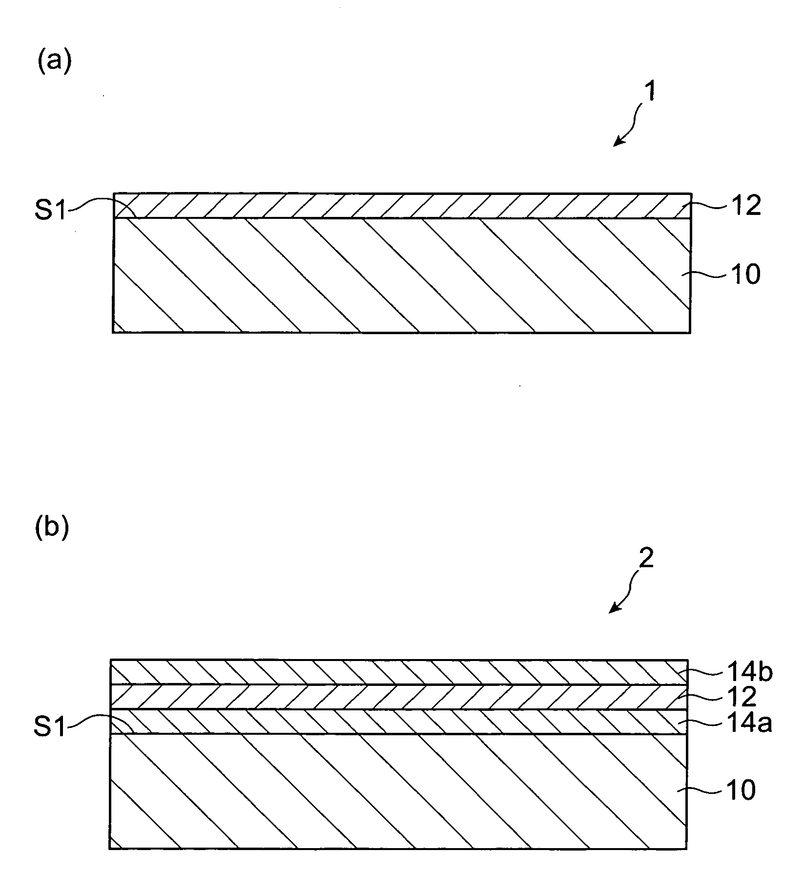
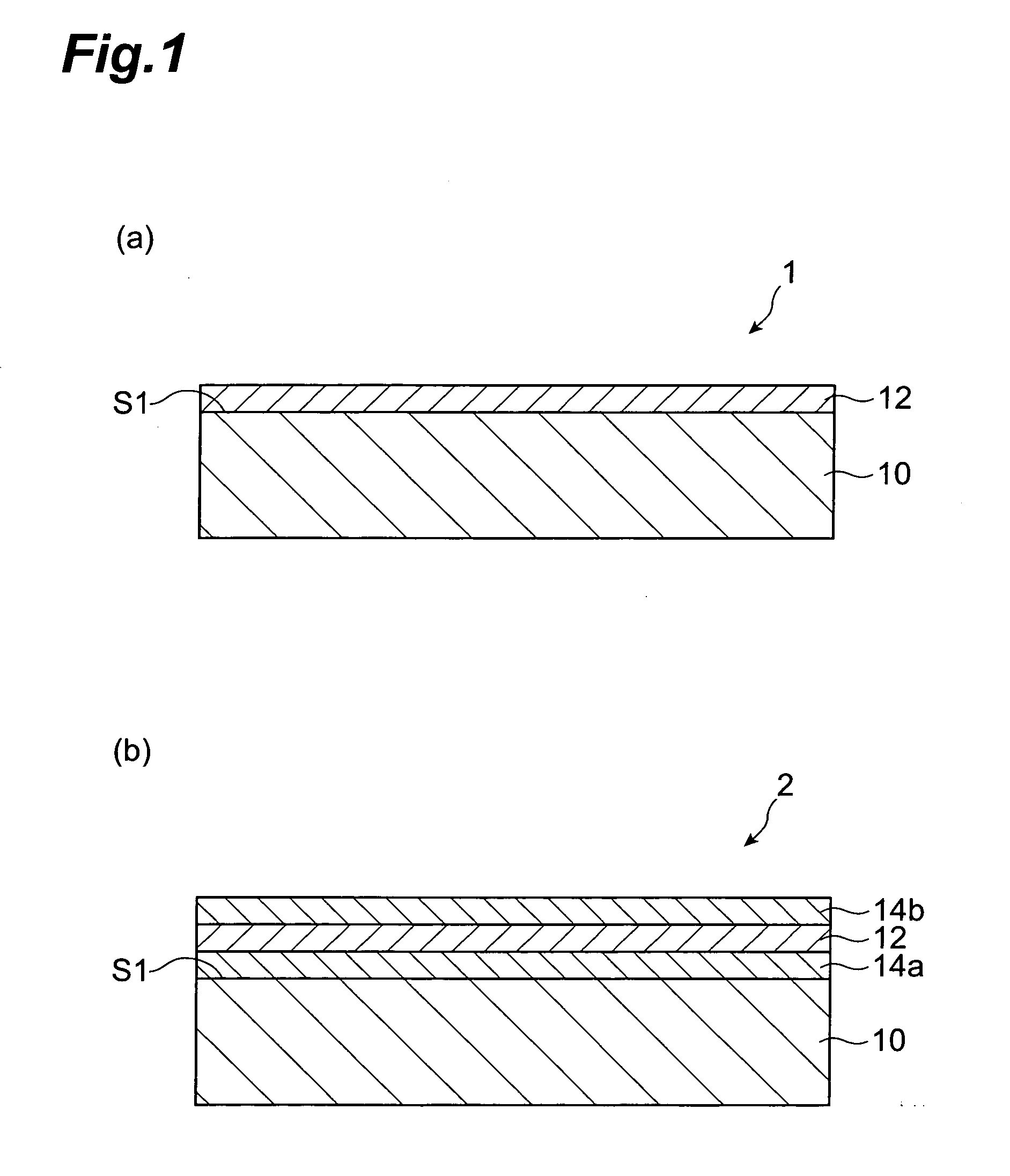
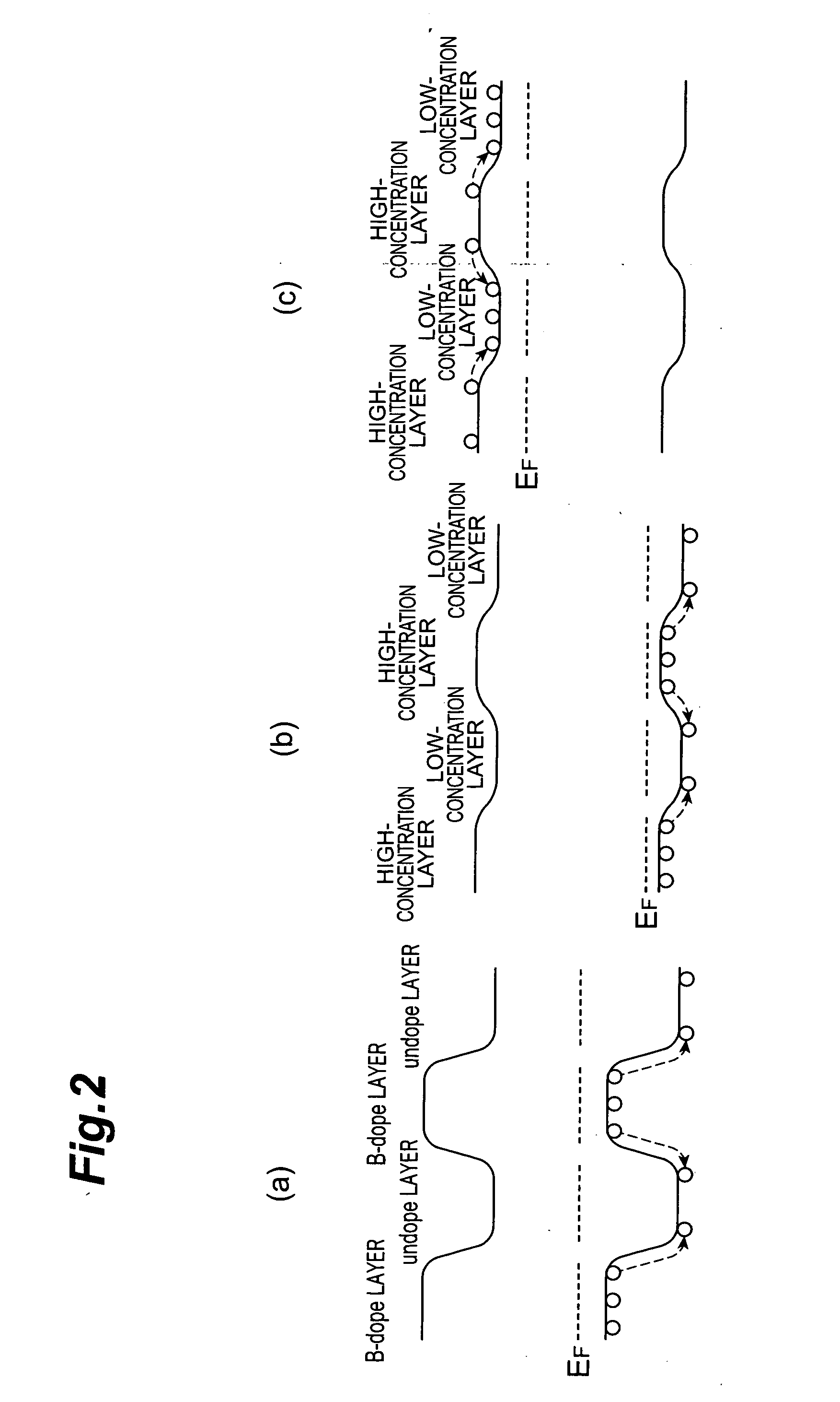
[0039] The present invention realizes a diamond n-type semiconductor in which the amount of change in carrier concentration is fully reduced in a wide temperature range, a method of manufacturing the same, and a semiconductor device and electron emitting device using the diamond n-type semiconductor.

Problems solved by technology

However, there are many wide-gap materials which cannot realize low-resistance n- and p-type layers.
In this case, low contact resistance cannot be realized.
If their carrier concentration is low, however, electrons cannot fully be accumulated even when biased, so that the bias applying effect cannot be utilized effectively, whereby electron emissions cannot be made easier.
In diamond, high-concentration doping of n-type semiconductors has been difficult, while very-high-concentration doping of p-type semiconductors has been easy.
Though low-concentration n-type semiconductors can be realized by P (phosphorus) doping or S (sulfur) doping, it has been very difficult to raise the doping concentration thereof.
Even when the crystallinity is kept, defects may occur.
High-concentration doping by ion implantation has been tried, but failed since the crystallinity has been very hard to restore because of irradiation damages caused by a high dosage of ion implantation.
In such a case, it is even uncertain whether the resulting diamond semiconductor is of n-type or not.
When diamond breaks down its crystallinity or incurs a defect, however, a pi bond may occur in carbon, thereby yielding metallic conduction even at a low resistance.

Method used


Image

  • Diamond N-Type Semiconductor, Method of Manufacturing the Same, Semiconductor Device, and Electron Emitting Device
  • Diamond N-Type Semiconductor, Method of Manufacturing the Same, Semiconductor Device, and Electron Emitting Device
  • Diamond N-Type Semiconductor, Method of Manufacturing the Same, Semiconductor Device, and Electron Emitting Device

Examples


specific example 1

[0072] Specific examples of the diamond n-type semiconductor, method of manufacturing the same, semiconductor, and electron emitting device according to the present invention will now be explained.

[0073] On a 2-mm square monocrystal diamond IIa {111} substrate, phosphorus-doped diamond was epitaxially grown under the following condition with a microwave plasma CVD apparatus having optimized its dopant gas introduction. The growing condition was such that the methane concentration (CH4 / H2)=0.003% to 1.0%, the phosphine concentration (PH3 / CH4)=1,000 ppm to 200,000 ppm, the power was 200 W to 400 W, the substrate temperature was 850° C. to 1,000° C., and the pressure was 100 Torr (1.33×10⁴ Pa). Further, a CO2 gas was added such that (CO2 / CH4)=0.1% to 10%. This was done in order to make the P take-up better than that in the case without CO2, though films will not be formed if CO2 is added by the same level as with CH4. As a consequence, an epitaxial film having a thickness of 1 to 2 μm...

specific example 2

[0085] In a method similar to that of Specific Example 1 mentioned above, Specific Example 2 yielded a diamond n-type semiconductor by synthesizing a phosphorus-doped layer doped with not only P but also Si as 50 ppm of an SiH4 gas (SiH4 / CH4). Separately, Specific Example 2 also yielded a diamond n-type semiconductor by synthesizing a phosphorus-doped layer while trying to mix Si therein by placing a solid supply source for Si (Si semiconductor substrate) near a diamond substrate. Unlike Specific Example 1, Specific Example 2 did not add a CO2 gas.

[0086]FIG. 8 is a table showing conditions under which phosphorus-doped layers (diamond semiconductor layers) were synthesized when Si was supplied by a gas, Si atom concentrations in SIMS results, and measurement results of Hall effect in a plurality of samples (diamond n-type semiconductors) manufactured. FIG. 9 is a table showing conditions under which phosphorus-doped layers were synthesized when Si was supplied by a solid, Si atom co...


PUM


Abstract

The present invention relates to a diamond n-type semiconductor in which the amount of change in carrier concentration is fully reduced in a wide temperature range. The diamond n-type semiconductor comprises a diamond substrate, and a diamond semiconductor formed on a main surface thereof and turned out to be n-type. The diamond semiconductor exhibits a carrier concentration (electron concentration) negatively correlated with temperature in a part of a temperature region in which it is turned out to be n-type, and a Hall coefficient positively correlated with temperature. The diamond n-type semiconductor having such a characteristic is obtained, for example, by forming a diamond semiconductor doped with a large amount of a donor element while introducing an impurity other than the donor element onto the diamond substrate.

Description

TECHNICAL FIELD [0001] The present invention relates to a diamond n-type semiconductor, a method of manufacturing the same, a semiconductor device employing the diamond n-type semiconductor, and an electron emitting device employing the diamond n-type semiconductor. BACKGROUND ART [0002] Power devices such as SCR, GTO, SIT, IGBT, and MISFET employing semiconductor materials have been manufactured while using n- and p-type semiconductors. It is important for these power devices to not only control their carrier concentrations, but also form a very high carrier concentration and lower their resistance. This is because their contact resistance to electrode metals for supplying a current is preferably as low as possible. Therefore, n+ and p+ layers have conventionally been formed by high-concentration doping, so as to realize an ohmic characteristic with a low resistance to metal layers through thus formed layers. The n+ and p+ layers may be formed by epitaxial growth or by forming a me...

Claims


Application Information

Patent Timeline
IPC IPC(8): H01L29/16H01L21/00H01J1/308
CPCH01L29/1602H01J1/308H01L29/16
Inventor NAMBA, AKIHIKONISHIBAYASHI, YOSHIKIIMAI, TAKAHIRO
Owner SUMITOMO ELECTRIC IND LTD
Learn More