Flip-Chip Mounting Method and Bump Formation Method

a technology of bump formation and flip-chip, which is applied in the direction of sustainable manufacturing/processing, final product manufacturing, semiconductor/solid-state device details, etc., can solve the problems of increasing the demands for reducing the dielectric constant, the difficulty of coping with this fine pitch, and the seriousness of rapid operation and power consumption loss, etc., to achieve easy quality control of the dipping bath, high wettability, and efficient incorporation

Active Publication Date: 2007-10-18
PANASONIC CORP
View PDF0 Cites 15 Cited by
  • Summary
  • Abstract
  • Description
  • Claims
  • Application Information

AI Technical Summary

Benefits of technology

[0040] In the flip-chip mounting method of this invention, a semiconductor chip and a circuit board held with a given gap provided therebetween are dipped in a dipping bath containing a melted resin including melted solder particles, so that the melted solder particles dispersed in the melted resin can be constantly supplied to the gap between the semiconductor chip and the circuit board. Therefore, bond of the melted solder particles is uniformly proceeded in the gap. As a result, the melted solder particles uniformly grown self-assemble between connection terminals of the circuit board and electrode terminals of the semiconductor chip with high wettability, and hence, connectors for electrically connecting the electrode terminals and the connection terminals to each other can be uniformly formed.
[0041] Furthermore, when the semiconductor chip and the circuit board held with the given gap are dipped while being rocked in the dipping bath or while allowing the melted resin contained in the dipping bath to flow, the melted solder particles dispersed in the melted resin can be more forcedly supplied to the gap between the semiconductor chip and the circuit board, and hence, the bond of the melted solder particles can be uniformly proceeded in a balanced manner. As a result, more uniform connectors can be formed between the electrode terminals and the connection terminals. In addition, since the melted solder particles dispersed in the melted resin can be efficiently incorporated into the gap, the ratio of the melted solder particles to be included in the melted resin can be set to be small, and hence, quality control of the dipping bath can be easily performed.
[0042] Moreover, after forming the connectors between the terminals of the circuit board and the semiconductor chip in the dipping bath, the circuit board and the semiconductor chip are taken out of the dipping bath and the melted resin having permeated into the gap between the circuit board and the semiconductor chip is cured. Thus, electric connection between the semiconductor chip and the circuit board and fixation of the semiconductor chip on the circuit board can be both performed through a series of procedures, and therefore, flip-chip mounting with high productivity can be realized.

Problems solved by technology

However, in order to mount a next generation LSI including electrode terminals in the number exceeding 5,000 on a circuit board, it is necessary to form bumps correspondingly to a fine pitch of 100 μm or less, but it is difficult to cope with this fine pitch by the current solder bump forming technology.
Therefore, problems of a rapid operation and a power consumption loss have become serious, and there are increasing demands for reducing the dielectric constant (i.e., attaining low-k) of an insulating film provided between interconnect layers.
The low-k of such an insulating film can be realized by making the material for the insulating film porous, and therefore, such a film is poor in the mechanical strength and hence is an obstacle to thickness reduction of a semiconductor.
Moreover, in the case where electrode terminals are formed in the area array arrangement, since the porous film has a problem of the strength due to its low-k, it is difficult to form bumps on the electrode terminals in the area array arrangement and to perform the flip-chip mounting itself.
Although the plating method is suitable for attaining a fine pitch, the process is complicated and is disadvantageous in the productivity.
Alternatively, the screen printing method is good at productivity but is not suitable for attaining a fine pitch because a mask is used.
However, in both of the techniques disclosed in Patent Documents 1 and 2, the paste composition is supplied onto the substrate through application, and hence, variation in thickness and concentration is locally caused.
Therefore, the amount of depositing solder is different among the electrodes, and hence, the bumps cannot be formed in a uniform height.
Also, in these methods, since the paste composition is supplied by the application onto the irregular surface of the circuit board where the electrodes have been formed, a sufficient amount of solder cannot be supplied onto the electrodes corresponding to convex portions, and therefore, it is difficult to attain a desired height of bumps necessary for the flip-chip mounting.

Method used


Image

  • Flip-Chip Mounting Method and Bump Formation Method
  • Flip-Chip Mounting Method and Bump Formation Method
  • Flip-Chip Mounting Method and Bump Formation Method

Examples


embodiment 1

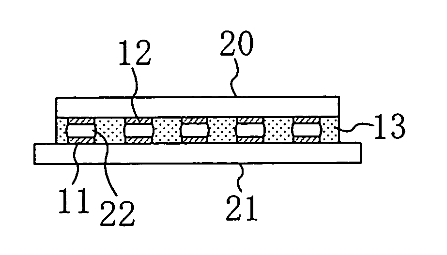
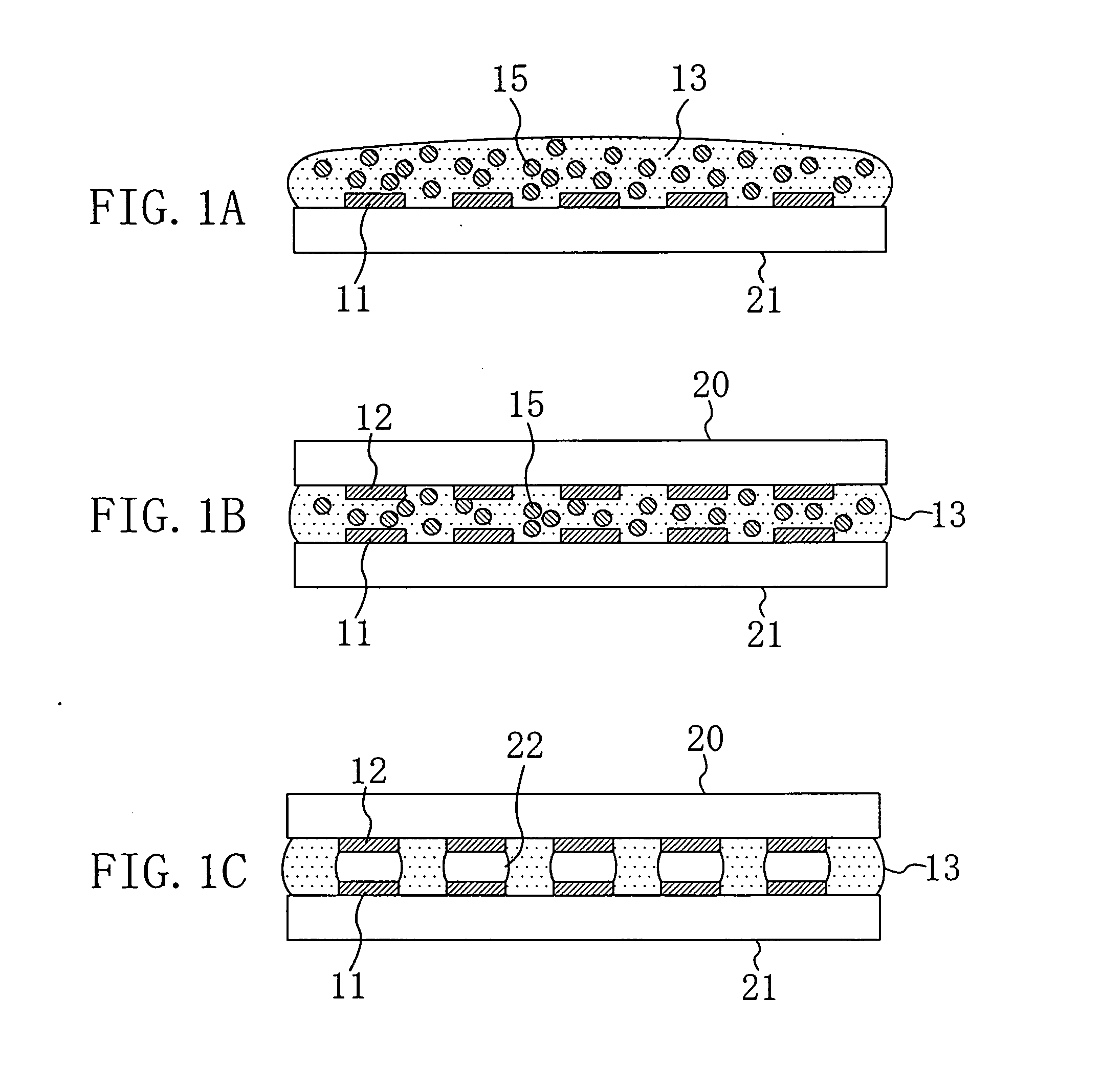
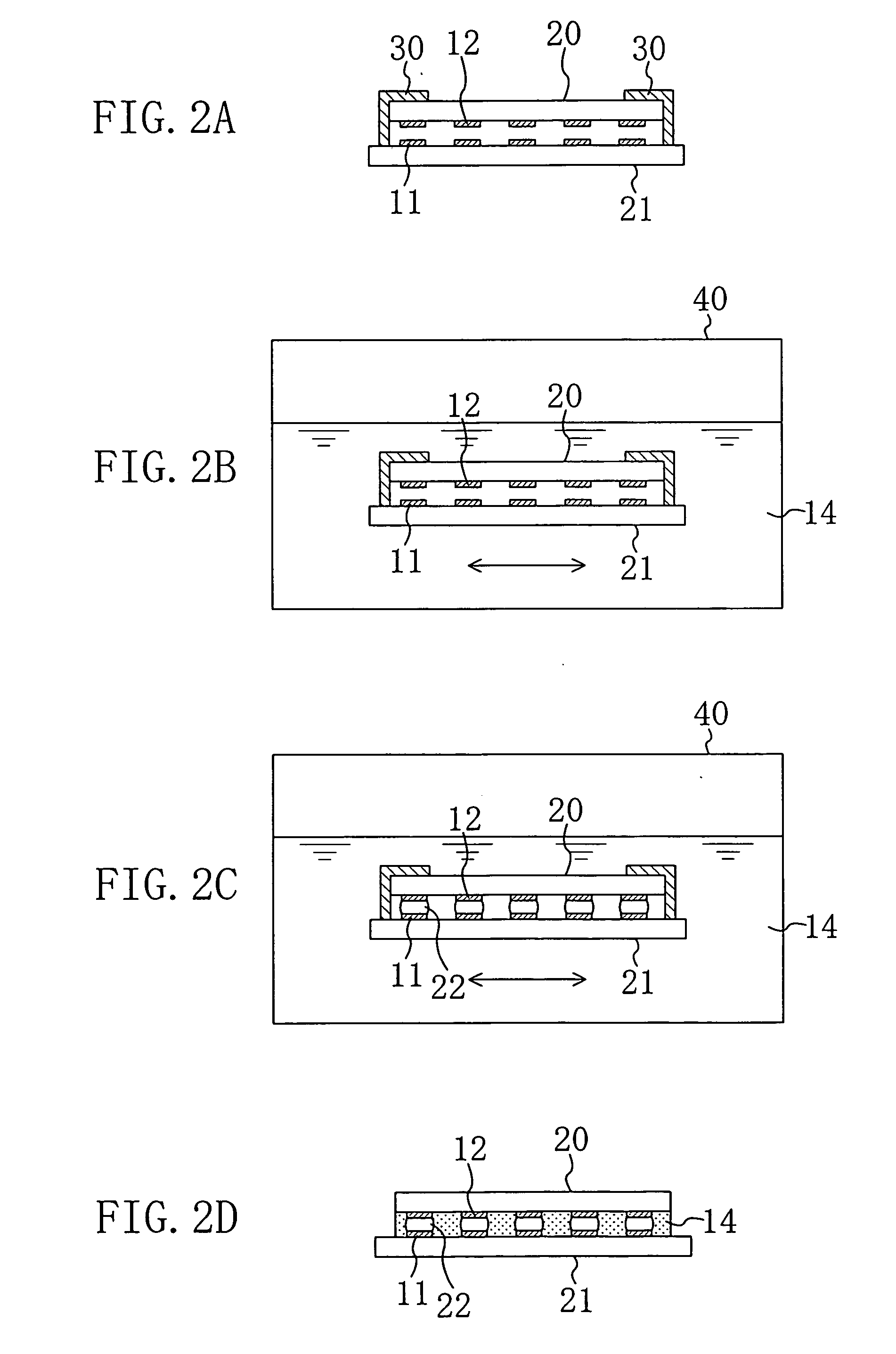
[0084]FIGS. 2a through 2d are cross-sectional views for showing basic procedures in a flip-chip mounting method according to Embodiment 1 of the invention.

[0085] First, as shown in FIG. 2A, a semiconductor chip 20 having a plurality of electrode terminals 12 is held by a fixing jig 30 so as to oppose a circuit board 21 having a plurality of connection terminals 11 with a given gap (of, for example, 10 through 100 μm) provided therebetween. At this point, the electrode terminals 12 of the semiconductor chip 20 and the connection terminals 11 of the circuit board 10 are aligned to oppose each other.

[0086] At this point, the fixing jig 30 may be anything as far as it can fix the semiconductor chip 20 and the circuit board 21 with the given gap provided therebetween, and a spacer may be inserted between the semiconductor chip 20 and the circuit board 21 for keeping the given gap.

[0087] Next, as shown in FIG. 2B, the semiconductor chip 20 and the circuit board 21 held with the given g...

embodiment 2

[0116] In the flip-chip mounting method described in Embodiment 1, a circuit board and a semiconductor chip are dipped in a dipping bath containing a melted resin including melted solder particles for a given period of time, so as to make the melted solder particles self-assemble between terminals of the circuit board and the semiconductor chip for forming connectors. This technique is also applicable to a bump formation method.

[0117]FIGS. 6A through 6D are cross-sectional views for showing basic procedures in a bump formation method according to Embodiment 2 of the invention. It is noted that detailed description of procedures commonly performed in the flip-chip mounting method shown in FIGS. 2A through 2D is omitted.

[0118] First, as shown in FIG. 6A, a substrate 25 having a plurality of electrodes 27 is held by a fixing jig 30 so as to oppose a flat plate 26 with a given gap (of, for example, 10 through 100 μm) provided therebetween.

[0119] Next, as shown in FIG. 6B, the substra...

embodiment 3

[0125]FIGS. 7 and 8 are diagrams of a mounting apparatus 50 used for executing the flip-chip mounting method of this invention.

[0126] The mounting apparatus 50 shown in FIG. 7 includes a fixing jig 30 for holding a semiconductor chip (not shown) and a circuit board (not shown) to oppose each other with a given gap provided therebetween, a dipping bath 40 containing a melted resin 14 including melted solder particles, and a conveyor 60 for conveying the fixing jig 30 into the dipping bath 40, and further includes annealing means 70 if necessary.

[0127] In this mounting apparatus 50, the fixing jig 30 holding the semiconductor chip and the circuit board is dipped in the dipping bath 40 by using the conveyor 60, so as to make the melted solder particles contained in the dipping bath 40 self-assemble between connection terminals of the circuit board and electrode terminals of the semiconductor chip, and thus, connectors are formed between these terminals.

[0128] The semiconductor chip ...


PUM

PropertyMeasurementUnit
temperatureaaaaaaaaaa
timeaaaaaaaaaa
grain sizeaaaaaaaaaa

Abstract

[Problem] To provide a flip-chip mounting method and a bump formation method applicable to flip-chip mounting of a next generation LSI and having high productivity and high reliability. [Means for Solving Problem] A semiconductor chip 20 having a plurality of electrode terminals 12 is held to oppose a circuit board 21 having a plurality of connection terminals 11 with a given gap provided therebetween, and the semiconductor chip 20 and the circuit board 21 in this state are dipped in a dipping bath 40 containing a melted resin 14 including melted solder particles for a given period of time. In this dipping process, the melted solder particles self-assemble between the connection terminals 11 of the circuit board 21 and the electrode terminals 12 of the semiconductor chip 20, so as to form connectors 22 between these terminals. Thereafter, the semiconductor chip 20 and the circuit board 21 are taken out of the dipping bath 40, and the melted resin 14 having permeated into the gap between the semiconductor chip 20 and the circuit board 21 is cured, so as to complete a flip-chip mounting body.

Description

TECHNICAL FIELD [0001] The present invention relates to a flip-chip mounting method for mounting a semiconductor chip on a circuit board and a method for forming a bump on an electrode of a substrate. BACKGROUND ART [0002] Recently, in accordance with the increased density and the increased degree of integration of semiconductor integrated circuits (LSIs) used in electronic equipment, the number of electrode terminals of an LSI chip has been rapidly increased and the pitch therebetween has been rapidly reduced. In mounting such an LSI chip on a circuit board, flip-chip mounting is widely employed for reducing interconnect delay. Generally, in the flip-chip mounting, solder bumps are formed on electrode terminals of an LSI chip and the electrode terminals of the LSI chip are connected as a whole to connection terminals formed on a circuit board through the solder bumps. [0003] However, in order to mount a next generation LSI including electrode terminals in the number exceeding 5,000...

Claims


Application Information

Patent Timeline
Patent Type & Authority Applications(United States)
IPC IPC(8): H05K3/34H01L21/00H01L21/44H05K3/00
CPCB23K35/0244Y10T29/53178H01L21/6835H01L24/11H01L24/12H01L24/16H01L24/75H01L2224/11003H01L2224/13099H01L2224/16H01L2224/75H01L2224/83886H01L2924/01002H01L2924/01004H01L2924/01009H01L2924/01011H01L2924/01013H01L2924/01015H01L2924/0103H01L2924/01032H01L2924/01033H01L2924/01047H01L2924/01056H01L2924/01078H01L2924/01082H01L2924/10329H01L2924/14H01L2924/30105H05K3/323H05K3/3436H05K3/3484H05K2201/10977H05K2203/1361H01L2924/01005H01L2924/01006H01L2924/01019H01L2924/0105H01L2924/014H01L2224/1131H01L21/563H01L2924/18161H01L2224/1319H01L2224/133H01L21/67144H01L2224/83815H01L2224/8321H01L24/83H01L2224/83192H01L2924/00014H01L2224/05573H01L2224/05568H05K3/3485Y02P70/50H01L2224/05599
Inventor HIRANO, KOICHIKARASHIMA, SEIJIICHIRYU, TAKASHITOMITA, YOSHIHIRONAKATANI, SEIICHI
Owner PANASONIC CORP
Why Eureka
Try Eureka