
High-Power Optoelectronic Device with Improved Beam Quality Incorporating A Lateral Mode Filtering Section

Inactive Publication Date: 2007-09-27
INNOLUME
View PDF0 Cites 37 Cited by
  • Summary
  • Abstract
  • Description
  • Claims
  • Application Information

AI Technical Summary

Benefits of technology

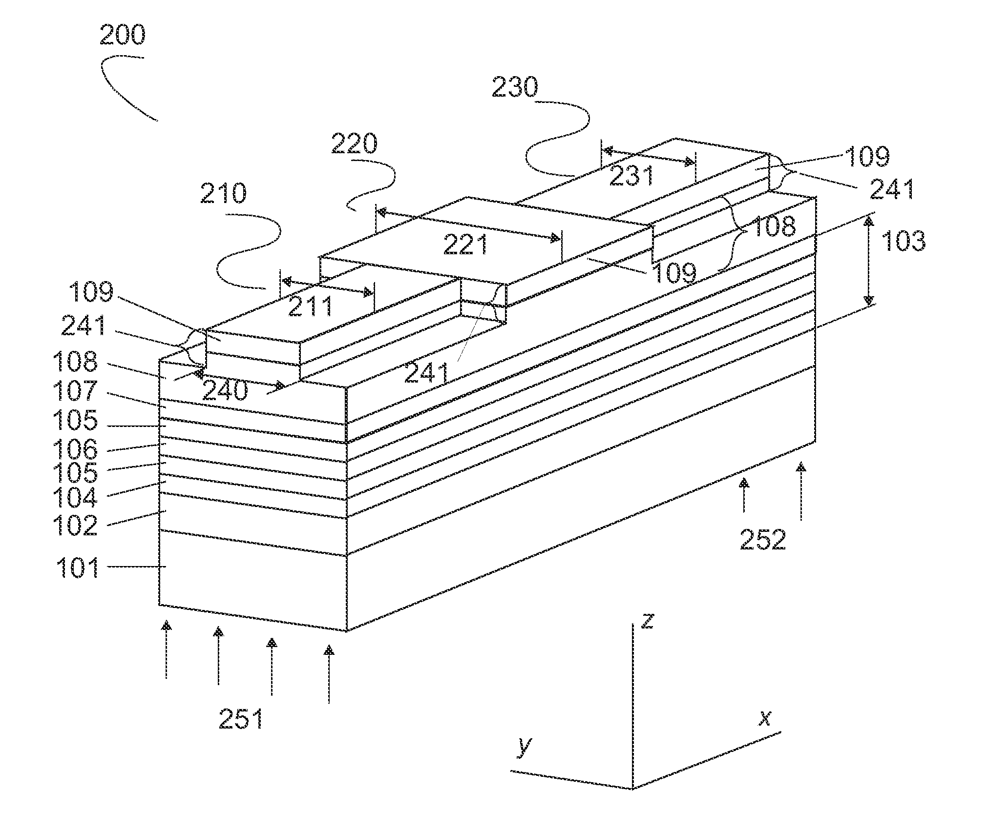
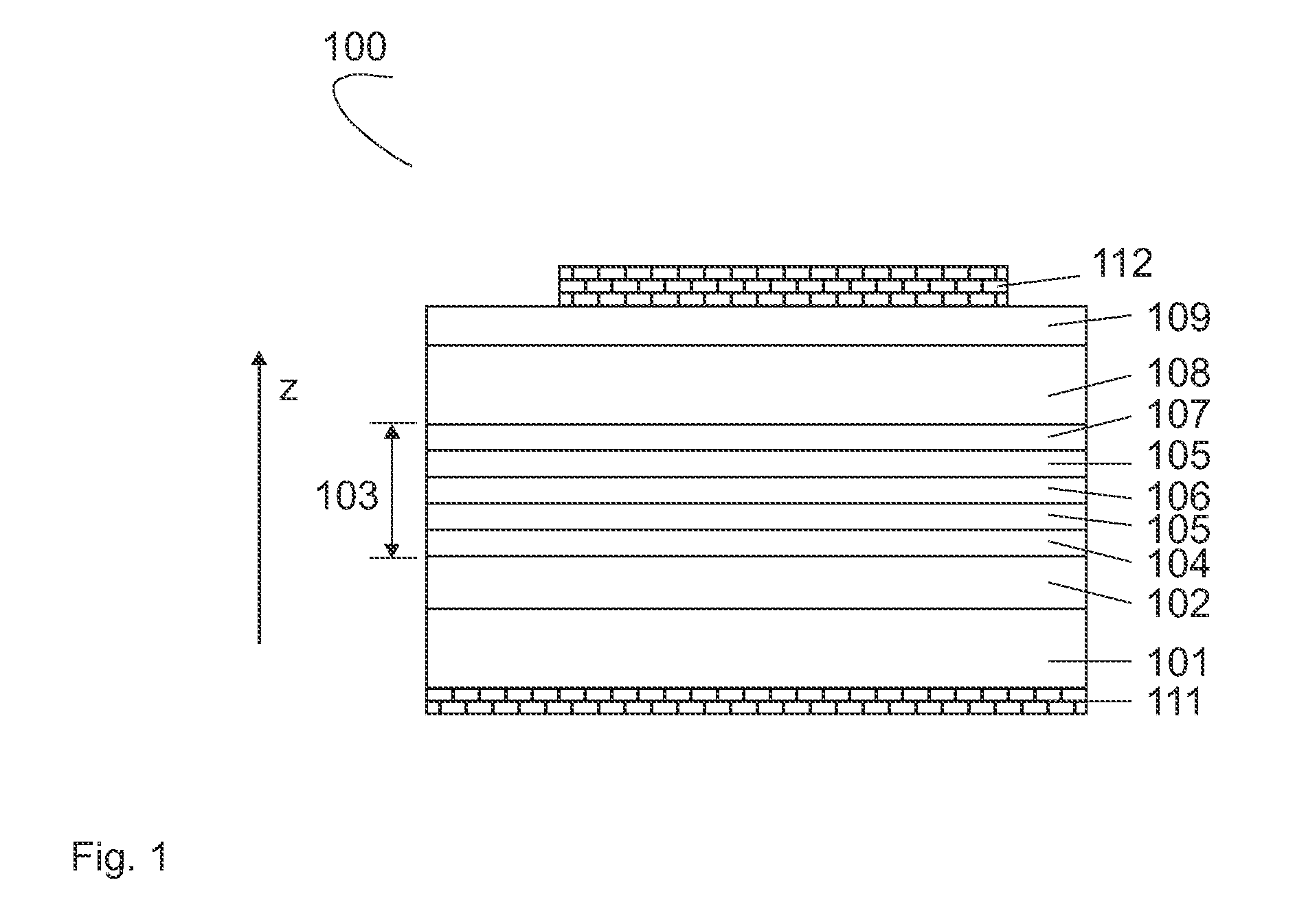
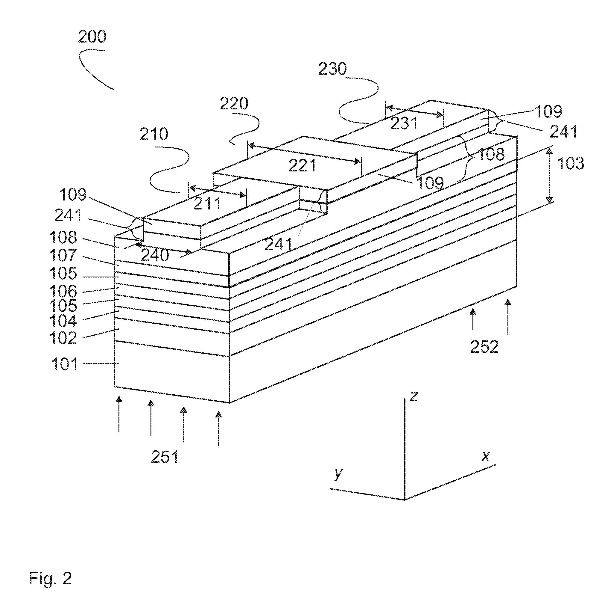
[0027] An optoelectronic device includes a planar active element, a vertical waveguide surrounding the active element in the vertical direction, and a lateral waveguide including at least one active section and at least one filter section following each other in the longitudinal direction. At least part of the active element within the active section generates optical gain in response to above-threshold pumping. The broad lateral waveguide in the active section can localize multiple lateral optical modes. In the filter section, no lateral confinement is provided for the lateral optical modes. The device further comprises means to ensure low absorption loss in the filter section and, therefore, ensure high efficiency. In one embodiment low absorption loss is achieved by pumping at least part of the active element within the filter section. In another embodiment the active element has small overlap with the vertical optical modes. The device operates as a single lateral mode optoelectronic device, possessing advantages of broad stripe optoelectronic devices.
[0028] The semiconductor optoelectronic device of the present invention includes a planar active element, the element being capable generating optical gain under appropriate pumping. The device is preferably based on one or more of various types of gain elements including, but not limited to, a bulk semiconductor layer, a quantum well, an array of quantum wires, an array of quantum dots, or any combination thereof. In one embodiment, the planar active element is a specially designed array of self-organized quantum dots. The optoelectronic device is free of the limitations and disadvantages of quantum well intermixing.
[0033] Therefore, leakage loss occurs for optical modes traveling along the filter section. Owing to the difference in effective lateral angles of propagation, higher leakage loss occurs for higher order optical modes. The lowest leakage loss occurs for the fundamental mode. The active section and the filter section are selected such that an amplification per path of the preselected lateral optical mode(s) is higher than an amplification per path for the lateral optical modes other than the preselected optical mode(s).
[0034] As a result, the device generates the reduced number of the lateral optical modes as compared to the number of the lateral optical modes, which can be localized in the active section of the lateral waveguide. Preferably, the device operates on the fundamental lateral mode as a single lateral mode optoelectronic device, possessing at the same time advantages of broad stripe optoelectronic devices.
[0035] The device further comprises means to ensure low absorption loss for propagating modes, the loss being caused by absorption of light by the active element in the filter section. This is achieved without any modification of the band gap of the active element by using quantum well intermixing. Owing to low absorption loss, high efficiency can be achieved.
[0036] In one embodiment, low absorption loss is achieved by pumping at least part of the active element within the filter section such that the active element within the filter section becomes nearly transparent for the propagating modes (the absorption loss caused by absorption of light by the planar active element within the filter section is low). To that end, in one embodiment, the device further comprises a second top contact mounted atop the filter section, electrically isolated from the first top contact. In another embodiment, the first and the second top contacts are electrically connected, but the total width of the second top contact is preferably narrower than the width of the first top contact.

Problems solved by technology

If the laser is a multimode device, each mode has a different far field pattern and a different efficient focus distance, thus making it impossible to focus the emitted laser light into a single spot.
This method, however, is incapable of avoiding the excitation of higher-order modes.
A disadvantage of these methods, however, is that the flared shape of the laser resonator (as opposed to a simple rectangular shape) requires a certain precision of the lithography, etching, and other steps in fabrication.
Its narrow width, however, which is typically a few microns, may cause additional difficulties in fabrication.
Moreover, narrow width of this region may result in worse heat dissipation as compared to broader sections, which may result in diode overheating and related unwanted effects.
A disadvantage of the method is additional complexity in the fabrication process due to a number of additional technological operations such as insulator deposition, photoresist deposition, photoresist etching, insulator etching, lift-off, absorbing layer deposition, and other technological steps.
Thus, for a round-trip pass, the higher order modes undergo a greater degree of diffraction and therefore experience higher losses than the fundamental mode.
However, quantum well intermixing is not always acceptable for optoelectronic devices.
Quantum well intermixing in its present form is limited to those devices which have a quantum well active region.
Quantum well intermixing is not applicable to lasers with a bulk active region because the bandgap of the bulk semiconductor material is practically insensitive to disordering of the potential profile as it is introduced by quantum well intermixing.
Lasers based on quantum wires are not yet well developed.
There is no reliable data as to whether or not a plane of self-organized quantum dots or a plane of quantum wires can be intermixed by a method similar to quantum well intermixing.
Also, a device fabricated by certain methods of quantum well intermixing can suffer from low external efficiency because of high loss in the intermixed sections.
Quantum well intermixing typically requires thermal annealing, which may have an undesired effect on the active region of the laser.
In particular, self-organized quantum dot lasers are known to be very sensitive to high-temperature treatment, and such a treatment can result in a significant unintentional shift of the lasing wavelength to a shorter wavelength (so-called, blue shift) in un-intermixed (active) sections of the laser.

Method used


Image

  • High-Power Optoelectronic Device with Improved Beam Quality Incorporating A Lateral Mode Filtering Section
  • High-Power Optoelectronic Device with Improved Beam Quality Incorporating A Lateral Mode Filtering Section
  • High-Power Optoelectronic Device with Improved Beam Quality Incorporating A Lateral Mode Filtering Section

Examples


Embodiment Construction

Filtering of Higher-Order Modes

[0061] A semiconductor optoelectronic device of the present invention exploits the filtering of higher order lateral modes. However, the device of the present invention does not use the quantum well intermixing required in U.S. Pat. No. 6,760,335, U.S. Patent Publication 2004 / 0120377 and the other prior art mentioned herein. The optoelectronic device may incorporate one or more of various types of gain elements. The optoelectronic device is free of the limitations and disadvantages of quantum well intermixing, which were discussed herein.

[0062] The following terms, as used throughout the present application, are defined as follows. The plane of the planar gain element is the (xy) plane, and the perpendicular direction is the z direction. Light propagates in the longitudinal direction (x). The direction (z) perpendicular to the planar gain element is termed the vertical direction. The lateral direction (y) is the direction perpendicular to both the l...


PUM


Abstract

An optoelectronic device includes a planar active element, a vertical waveguide surrounding the active element in the vertical direction, and a lateral waveguide comprising at least one active section and at least one filter section following each other in the longitudinal direction. At least part of the active element within the active section generates optical gain in response to above-threshold pumping. The broad lateral waveguide in the active section can localize multiple lateral optical modes. In the filter section, no lateral confinement is provided for the lateral optical modes. The device further comprises means to ensure low absorption loss in the filter section and, therefore, ensure high efficiency. In one embodiment low absorption loss is achieved by pumping of at least part of the active element within the filter section. In another embodiment, the active element has small overlap with the vertical optical modes.

Description

BACKGROUND OF THE INVENTION [0001] 1. Field of the Invention [0002] The invention pertains to the field of optoelectronic devices. More particularly, the invention pertains to semiconductor diode lasers and superluminescent light-emitting diodes operating in the single spatial mode regime. [0003] 2. Description of Related Art [0004] Semiconductor edge-emitting lasers are known in the art. In particular, single spatial mode edge-emitting lasers are known, which are capable of operating at the fundamental optical mode in both vertical and lateral directions. One advantage of a single spatial mode laser is a single lobe far field pattern and, as a result, the possibility for efficient coupling of the outgoing laser light into a single mode optical fiber or a single mode waveguide. If the laser is a multimode device, each mode has a different far field pattern and a different efficient focus distance, thus making it impossible to focus the emitted laser light into a single spot. This em...

Claims


Application Information

Patent Timeline
IPC IPC(8): H01S5/00
CPCG02B6/1228H01S5/026H01S5/0265H01S5/028H01S5/0425H01S5/0625H01S2301/18H01S5/0657H01S5/1014H01S5/16H01S5/22H01S5/50H01S5/0655H01S5/04256
Inventor LIVSHITS, DANIILKOVSH, ALEXEYZHUKOV, ALEXEY
Owner INNOLUME
Learn More