
Semiconductor circuit

a technology of semiconductors and circuits, applied in pulse generators, pulse techniques, instruments, etc., can solve the problems of lack of study, lack of study of charge-discharge capacitors, and inability to study methods, etc., to achieve low threshold voltage, improve reliability, and reduce size

Inactive Publication Date: 2007-09-20
HITACHI LTD
View PDF9 Cites 39 Cited by
  • Summary
  • Abstract
  • Description
  • Claims
  • Application Information

AI Technical Summary

Benefits of technology

[0010]According to one aspect of the invention, there is provided a semiconductor circuit including a negative power source voltage generating circuit utilizing the energy charged to a capacitor from the output terminal to reduce the number of power supplies for the controlling circuits. Further, according to this aspect of the invention, a voltage terminal is interposed between a high-voltage terminal and a reference voltage terminal and a negative power source voltage generating circuit is arranged between the voltage terminal and a plurality of output terminals.
[0011]According to another aspect of the invention, there is provided a semiconductor circuit including a high-voltage switch for controlling the advisability of applying a voltage to the high-voltage terminal, wherein even in the case where the high-voltage switch is turned off or the voltage for the controlling circuit of the power switching element drops with the reduction in the power supplied to the power switching element, the controlling circuit is operated by charging the power supply capacitor for the controlling circuit from the high-voltage terminal, thereby preventing an excessively large current from being supplied to the power switching element. As an alternative, in the case where the power supplied to the power supply of the controlling circuit of the power switching element is reduced, the gate voltage of the power switching element is automatically decreased to prevent an excessive current from flowing in the power switching element.
[0012]According to still another aspect of the invention, there is provided a semiconductor circuit, wherein in the case where the power supplied from the power supply for the controlling circuit of the power switching element is reduced, a current path is formed to reduce the voltage of the high-voltage terminal. Also, in order to reduce the power consumption of the controlling circuit of the power switching element, a switch to turn off the current to a logic controlling circuit unit in the controlling circuit is inserted in the case where the logic controlling circuit unit is not required to be operated. Further, in order to reduce the ratio dV / dt of the output voltage while preventing the output terminal voltage from considerably deviating from the voltage range of the voltage of the high-voltage terminal and the voltage at the reference voltage terminal at the time of rapid switching operation, a capacitor adapted for charge or discharge operation only in the neighborhood of the voltage of the high-voltage terminal and the voltage of the reference voltage terminal is connected to the output terminal.
[0015]According to this invention, the controlling circuit of the normally-on switching element or the normally-off switching element having a low threshold voltage can be simplified and the semiconductor circuit reduced in size while at the same time improving the reliability. Also, the circuit configuration according to the invention realizes a low-loss, high-speed soft switching operation.

Problems solved by technology

The prior art described in JP-A-2004-304527, on the other hand, lacks the study of a method to charge the power supply capacitor of the upper-arm switching element through the upper-arm switching element.
Further, JP-A-2004-304527, in spite of the study being made about charging the power supply capacitor of the upper-arm switching element from an auxiliary capacitor using three sets of charge-discharge switching elements and auxiliary capacitors, fails to study the method of reducing the number of the charge-discharge capacitors.
Nevertheless, the study is not made about turning off the switching element in collaboration between the switch circuit and a protective circuit and the manner in which the switching element is turned off.

Method used


Image

  • Semiconductor circuit
  • Semiconductor circuit
  • Semiconductor circuit

Examples


embodiment 1

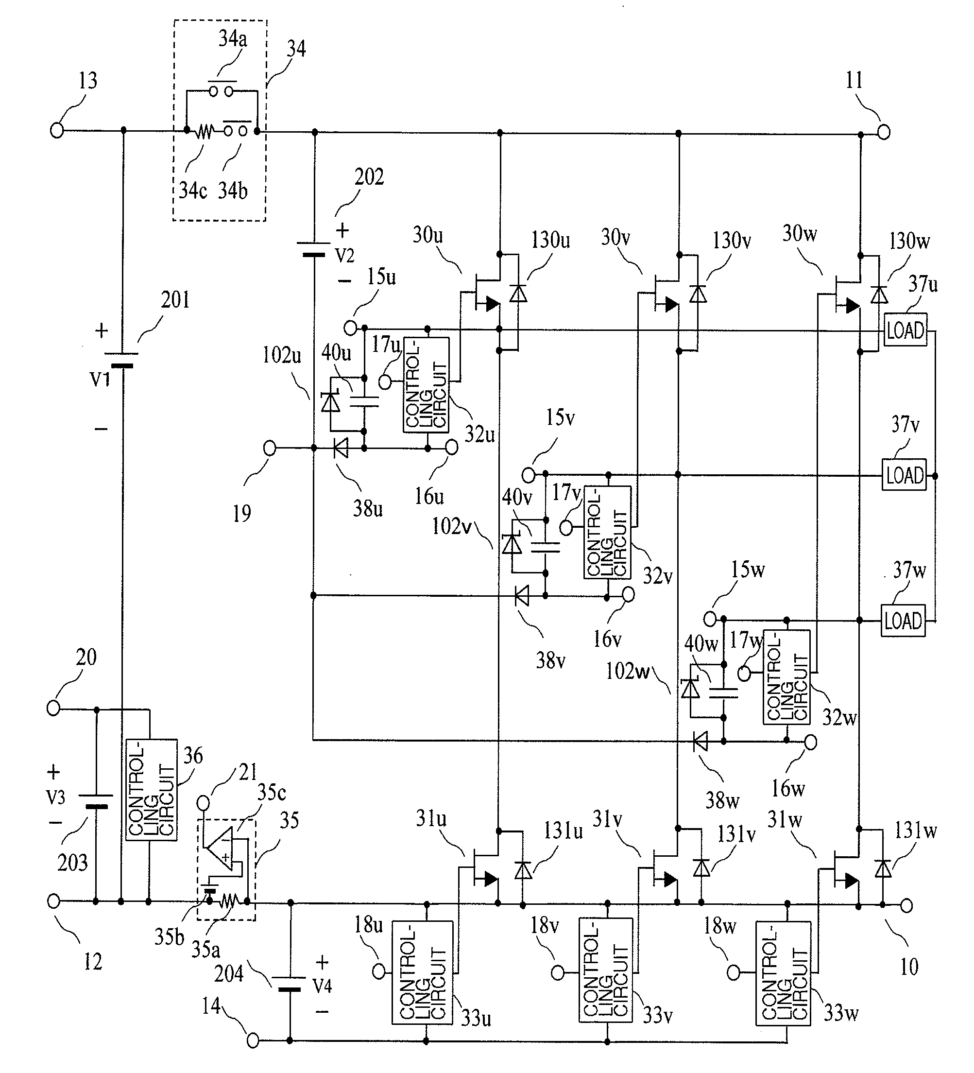
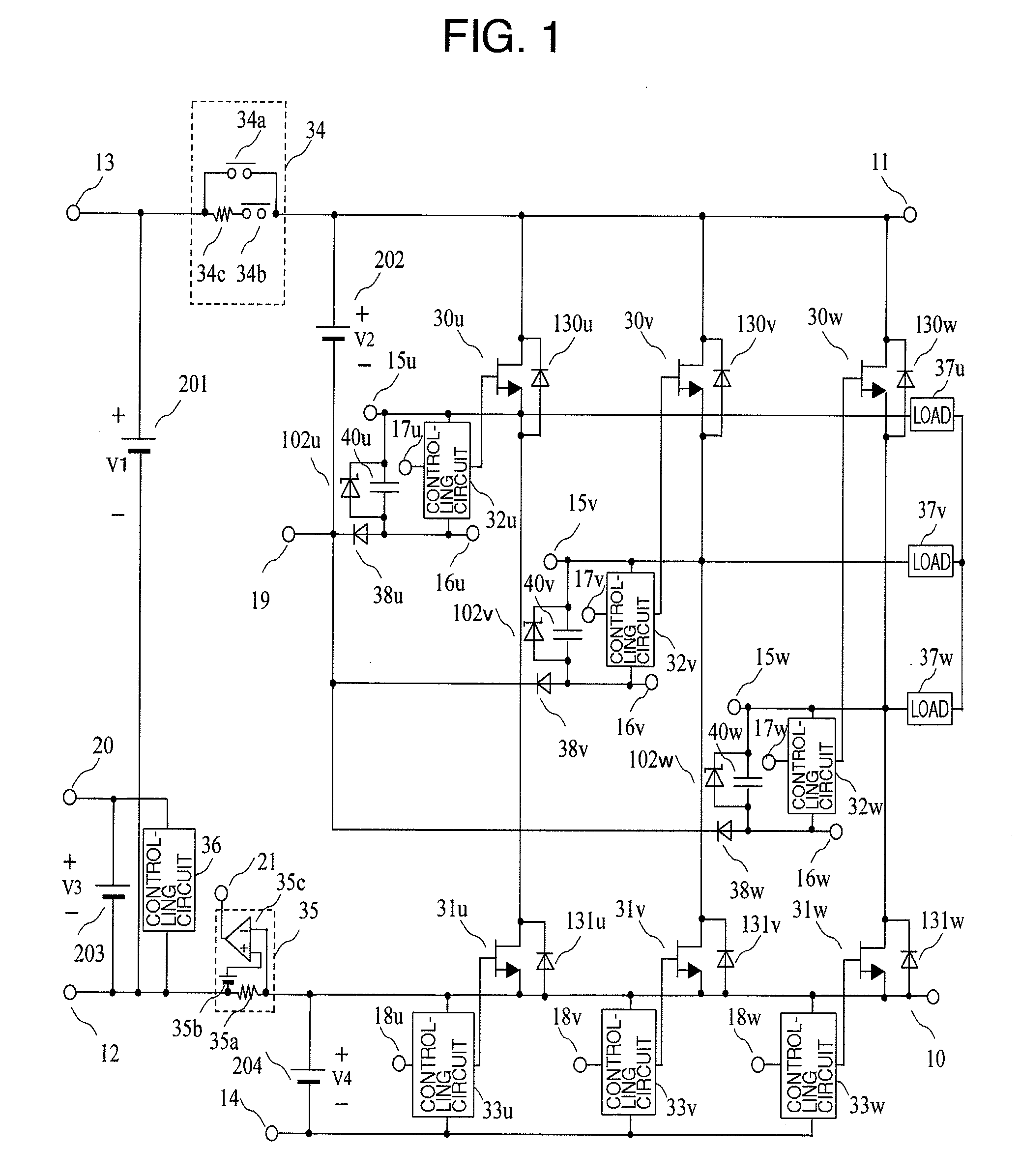
[0052]FIG. 1 is a diagram for explaining a semiconductor circuit according to a first embodiment. This embodiment represents a circuit using a n-channel JFET for the upper-arm switching elements 30u, 30v, 30w and the lower-arm switching elements 31u, 31v, 31w. Nevertheless, field-effect switching elements or a bipolar transistor other than JFET such as SIT, MESFET, HFET, HEMT or accumulation type FET may be used with equal effect. This embodiment is explained taking the normally-on switching elements 30u, 30v, 30w, 31u, 31v, 31w as an example.

[0053]This embodiment represents a three-phase inverter configured of a bridge circuit wherein the upper-arm switching elements 30u, 30v, 30w are connected between the high-voltage terminal 11 and the high-voltage-side voltage terminals 15u, 15v, 15w providing output terminals, the lower-arm switching elements 31u, 31v, 31w are arranged between the high-voltage-side voltage terminals 15u, 15v, 15w providing output terminals and the reference vo...

embodiment 2

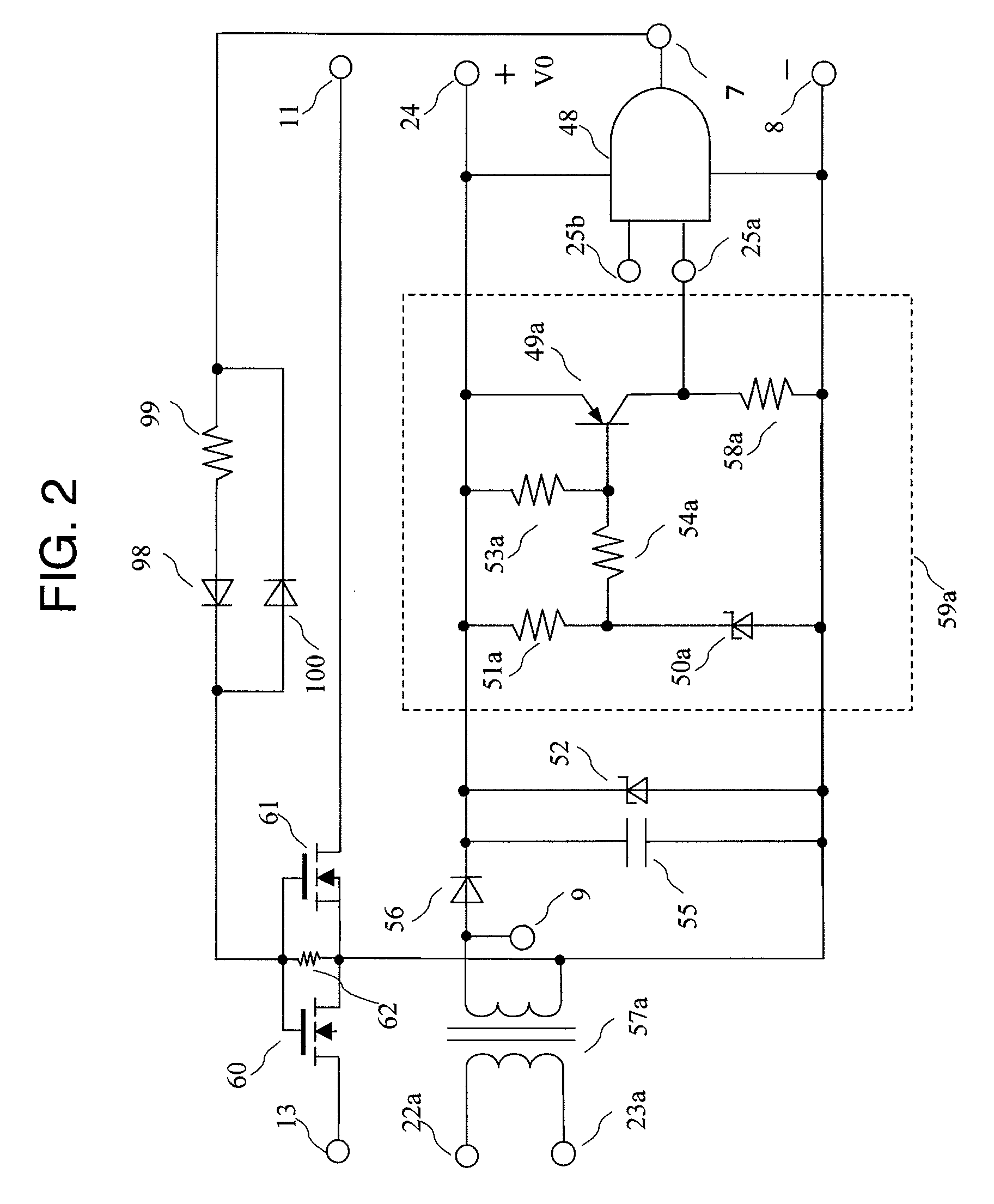
[0077]FIG. 2 is a diagram for explaining a semiconductor circuit according to a second embodiment. According to this embodiment, the high-voltage switch 34 shown in FIG. 1 is formed of normally-off power MOSFETs 60, 61 as semiconductor switching elements. FIG. 2 shows a bidirectional switch in which the normally-off power MOSFET 60 and the normally-off power MOSFET 61 are connected in series in opposite directions. As a result, the reverse flow to the input-side high-voltage terminal 13 from the high-voltage terminal 11 can be prevented at the time of turning off the high-voltage switch 34. In the case where the reverse flow prevention is not required, the normally-off power MOSFET 61 is eliminated. According to this embodiment, the voltage applied to the primary terminals 22a, 23a of the transformer 57a is transmitted to the secondary terminals 9, 8, and shaped by the capacitor 55 and the diode 56 thereby to generate the DC voltage V0 of about 10 V between the terminals 24 and 8.

[0...

embodiment 3

[0081]FIG. 3 is a diagram for explaining the semiconductor circuit according to a third embodiment. This embodiment represents a case in which the power supplies 202, 204 shown in FIG. 1 are formed of a rectifying circuit including a transformer 57a, capacitors 64a, 64b, diodes 65a, 65b and zener diodes 63a, 63b. Nevertheless, the power supplies 202, 204 may be implemented with a DC / DC power supply. In FIG. 3, numerals 59b, 59c designate a comparator circuit which, like the circuit 59a in FIG. 2, has a reference voltage equal to the breakdown voltage value of the zener diodes 50b, 50c to determine whether the power source voltages V2, V4 have reached the desired voltage level. In the state free of the effects of the parasitic inductance or the parasitic resistance of the wiring, the power source voltages V2, V4 are set to about 25V to 40 V in the case where the threshold voltage of the switching elements 30u, 30v, 30w, 31u, 31v, 31w is −20 V. Accordingly, the breakdown voltage of th...


PUM


Abstract

A semiconductor circuit suitable for normally-on switching elements or switching elements low in threshold voltage. A negative power supply is charged by a high-voltage power supply. A high-voltage switch controls the advisability of applying a voltage to a high-voltage terminal. With deducing the power supply to power switching elements, the high-voltage switch is turned off, and even in the case where the voltage of the controlling circuits of the power switching elements is reduced, the power supply capacitors for the controlling circuits are charged by the high-voltage terminal thereby to operate the controlling circuits. Further, a negative power source voltage generating circuit utilizes the energy charged to the capacitors from output terminals. A voltage terminal is inserted between the high-voltage terminal and a reference voltage terminal. The negative power source voltage generating circuit is interposed between the voltage terminal and a plurality of the output terminals.

Description

BACKGROUND OF THE INVENTION[0001]This invention relates to a semiconductor circuit suitable for a normally-on semiconductor switching element turned on even in the case where the gate voltage is zero volt and a normally-off semiconductor switch having a low threshold voltage.[0002]Although a wide band gap semiconductor element of such a material as SiC (carbon silicate), GaN (gallium nitride) or diamond has superior characteristics as a switching element, a typical semiconductor element using this wide band gap semiconductor element such as a junction type FET (hereinafter referred to as JFET), a static induction type transistor (hereinafter referred to as SIT), a metal-semiconductor-field-effect-transistor (hereinafter referred to as MESFET), a heterojunction field effect transistor (hereinafter referred to as HFET), a high electron mobility transistor (hereinafter referred to as HEMT) or an accumulation type FET has a normally-on characteristic with the drain current flowing even ...

Claims


Application Information

Patent Timeline
Patent Type & Authority Applications(United States)
IPC IPC(8): G05F1/00
CPCH03K17/063
Inventor SAKAMOTO, KOZO
Owner HITACHI LTD
Learn More