Formation of metal oxide nanowire networks (nanowebs) of low-melting metals
- Summary
- Abstract
- Description
- Claims
- Application Information
AI Technical Summary
Benefits of technology
Problems solved by technology
Method used
Image
Examples
example 1
[0089] Commercially available gallium oxide powder (Alfa Aesar) was dispersed in acetone and ultrasonicated for 2 minutes. Five drops of the well-dispersed suspension were then dropped on a 1 cm×1 cm quartz substrate and allowed to dry naturally. The resulting deposit on the substrate constituted a dense packed agglomerate of polycrystalline gallium oxide particles. (SEM showed precursor particles ranged from 50-300 microns). The gallium oxide film was then exposed to hydrogen plasma followed by hydrogen-oxygen plasma. The plasma treatments were done in a microwave plasma reactor (ASTEX 5010) at the following range of process conditions: Microwave power of 500-1200 W, pressure of 20-60 Torr, 2-30 minutes of hydrogen plasma treatment, 15 minutes to 3 hours of plasma treatment to a mixture of hydrogen and oxygen (0.6 20 sccm O2 / 100 sccm in the feed gas). The substrate temperature was measured using an infrared pyrometer to be approximately 550° C. for 700 W microwave power, 40 Torr to...
example 2
Two-dimensional Nanostructures: Nanowire Networks (Nanowebs)
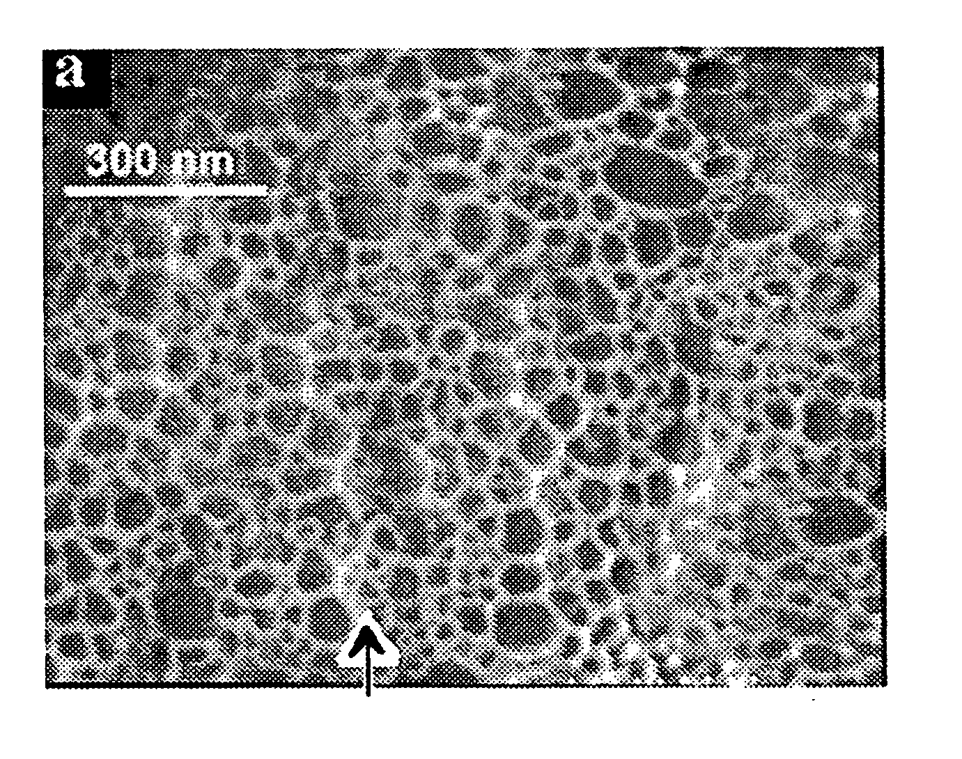
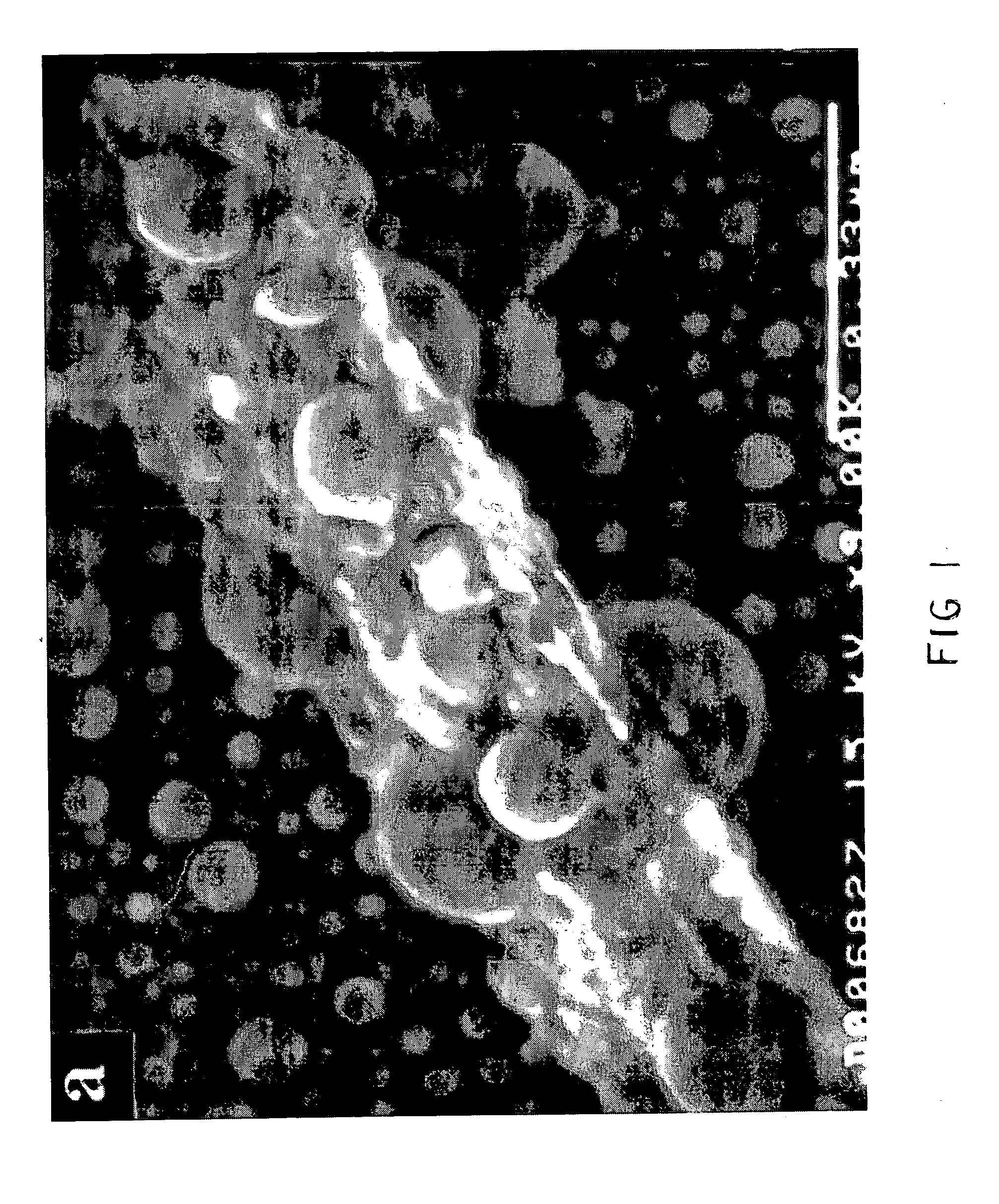
[0090] The small clusters (<100 nm) of Ga tend to flatten out with exposure to wetting gas phase species such as nitrogen or oxygen. The nanowires nucleating from these small clusters tend to grow parallel to the substrate and physically impinge on each other. The schematic of FIG. 17 shows nanoweb formation. The studies using oxygen and hydrogen in the gas phase over small clusters of Ga over quartz substrate led to the formation of two-dimensional network of nanowires. The individual segments of the network were on the order of few nm (<10 nm). The entire process is rapid and takes place within few minutes over large areas. The gallium oxide nanoweb is shown as a high -resolution WEM image and high-resolution TEM image as shown in FIGS. 18 and 19, respectively.
[0091] It is contemplated that electrical contacts can be formed to large area nanowire networks and used for sensors (tin oxide and zinc oxide). It is expected t...
PUM
 Abstract
Description
Claims
Application Information
 - R&D
- Intellectual Property
- Life Sciences
- Materials
- Tech Scout
- Unparalleled Data Quality
- Higher Quality Content
- 60% Fewer Hallucinations
Browse by: Latest US Patents, China's latest patents, Technical Efficacy Thesaurus, Application Domain, Technology Topic, Popular Technical Reports.
© 2025 PatSnap. All rights reserved.Legal|Privacy policy|Modern Slavery Act Transparency Statement|Sitemap|About US| Contact US: help@patsnap.com


