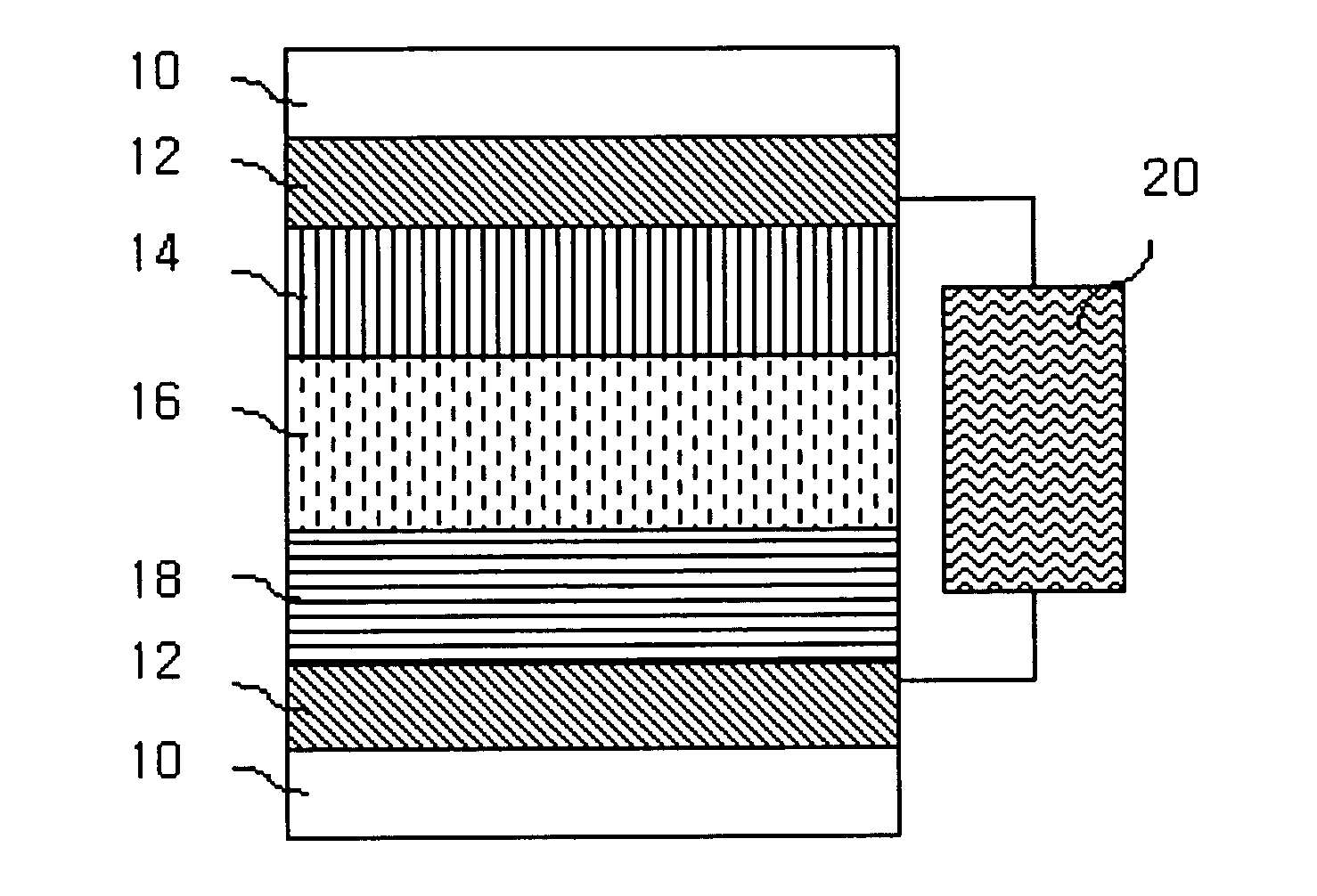
Electrochromic device comprising protective inorganic solid electrolyte film and manufacturing method thereof
a technology of inorganic solid electrolyte film and electrolyte film, which is applied in the direction of instruments, non-linear optics, optics, etc., can solve the problems of reversible intercalation and deintercalation, deterioration of properties, and stability problems of prior electrochromic devices, so as to improve device properties, improve durability, and improve the effect of memory
- Summary
- Abstract
- Description
- Claims
- Application Information
AI Technical Summary
Benefits of technology
Problems solved by technology
Method used
Image
Examples
example 1
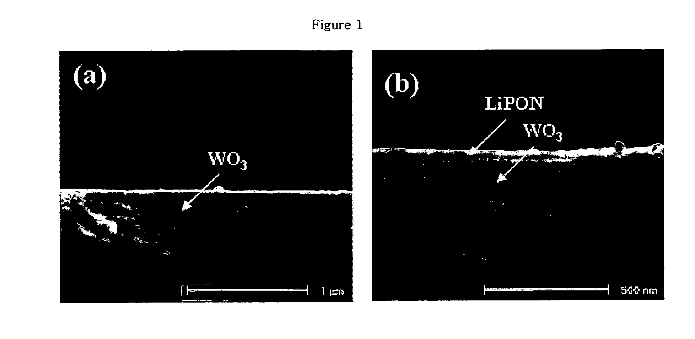
[0050] On glass substrates each having a transparent electrode (ITO) coated thereon while interposing 30-nm-thick silicon oxide (SiO2) there between, WO3 was deposited on the transparent electrode (ITO) in a vacuum of 10 mTorr at room temperature under an argon atmosphere at an RF power of 100 W for 90 minutes. The deposition rate of the tungsten oxide was 4.4 nm / min. WO3 was deposited to a thickness of about 400 nm. Then, on the WO3 layer, LiPON (Li3.3PO3.8NO0.22, United Vacuum & Materials (UVM)) was deposited. A LiPON target was used as an inorganic solid electrolyte, and the distance between the transparent electrode substrate and the LiPON target was 25 cm. The pressure before starting the experiment was 2.5×10⁻⁶ Torr, and the sputtering operation was carried out in a pressure of 10×10−3 Torr at room temperature in a nitrogen atmosphere at a power of 100 W for 30 minutes. The deposition rate of LiPON was 1.6 nm / min, and as shown in FIG. 1b, LiPON was deposited to a thickness of ...
example 2
[0052] The procedure of Example 1 was repeated except for RF power and deposition time, thus manufacturing devices consisting each of substrate (glass) / transparent electrode layer (ITO) / electrochromic layer (WO3) / protective inorganic solid electrolyte film (LiPON), in which the thicknesses of the inorganic solid electrolyte films of the devices were 10 nm, 32 nm, 50 nm, 98 nm, and 199 nm, respectively. The thickness of each of the inorganic solid electrolyte films increased with increases in RF power and deposition time, and a scanning electron microscope photograph of the electrochromic layer (WO3) and the protective inorganic solid electrolyte film (LiPON) in each of the devices is shown in FIG. 8.
PUM
| Property | Measurement | Unit |
|---|---|---|
| thickness | aaaaa | aaaaa |
| thickness | aaaaa | aaaaa |
| thickness | aaaaa | aaaaa |
Abstract
Description
Claims
Application Information
 - R&D
- Intellectual Property
- Life Sciences
- Materials
- Tech Scout
- Unparalleled Data Quality
- Higher Quality Content
- 60% Fewer Hallucinations
Browse by: Latest US Patents, China's latest patents, Technical Efficacy Thesaurus, Application Domain, Technology Topic, Popular Technical Reports.
© 2025 PatSnap. All rights reserved.Legal|Privacy policy|Modern Slavery Act Transparency Statement|Sitemap|About US| Contact US: help@patsnap.com


