Semiconductor fabrication and structure for field-effect and bipolar transistor devices

a technology of bipolar transistors and semiconductors, applied in the field of semiconductor devices, to achieve the effect of enhancing the properties of semiconductor devices

Inactive Publication Date: 2005-03-17
BIOTA
View PDF7 Cites 2 Cited by
  • Summary
  • Abstract
  • Description
  • Claims
  • Application Information

AI Technical Summary

Benefits of technology

[0008] In making a p-type device region on a semiconductor wafer, an initial semiconductor device region is defined by a buried region, and an initial spreading resistivity profile is developed by annealing. I have discovered that, after annealing, semiconductor device properties can be enhanced by removing a surface sub-region of the initial device region, and can be further improved by epitaxially growing thereon a monocrystalline film as an improved channel layer for FET devices. Such properties are relevant in MOS as well as bipolar devices.

Problems solved by technology

Such materials are disadvantaged, however, in having a large dose of oxygen ions implanted through the top surface layer of a silicon wafer on which devices are fabricated.

Method used


Image

  • Semiconductor fabrication and structure for field-effect and bipolar transistor devices
  • Semiconductor fabrication and structure for field-effect and bipolar transistor devices
  • Semiconductor fabrication and structure for field-effect and bipolar transistor devices

Examples


Embodiment Construction

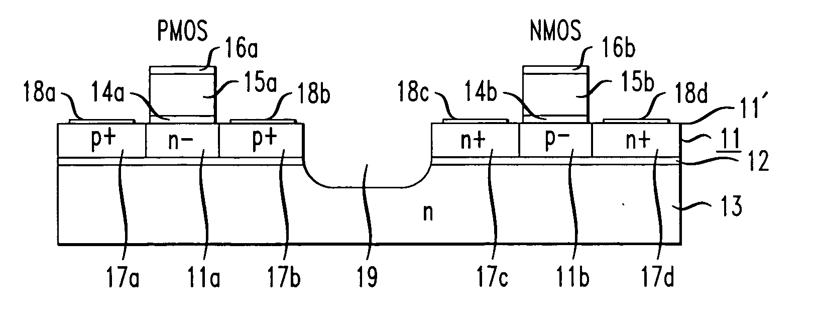
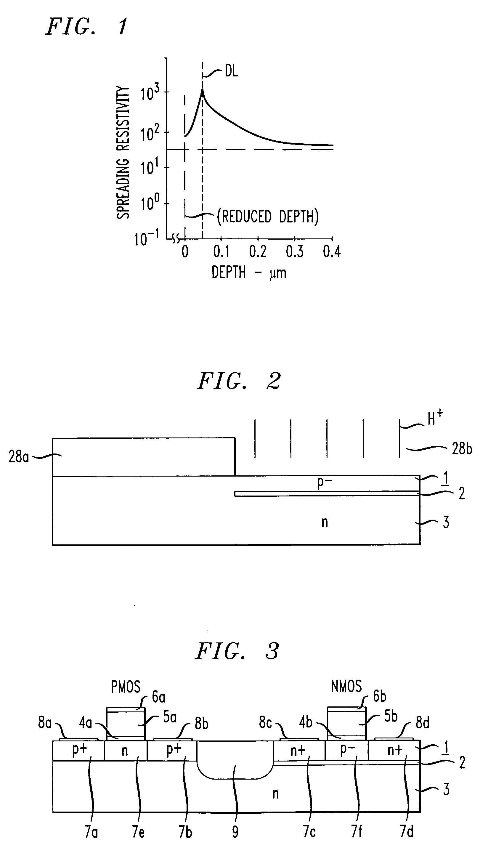
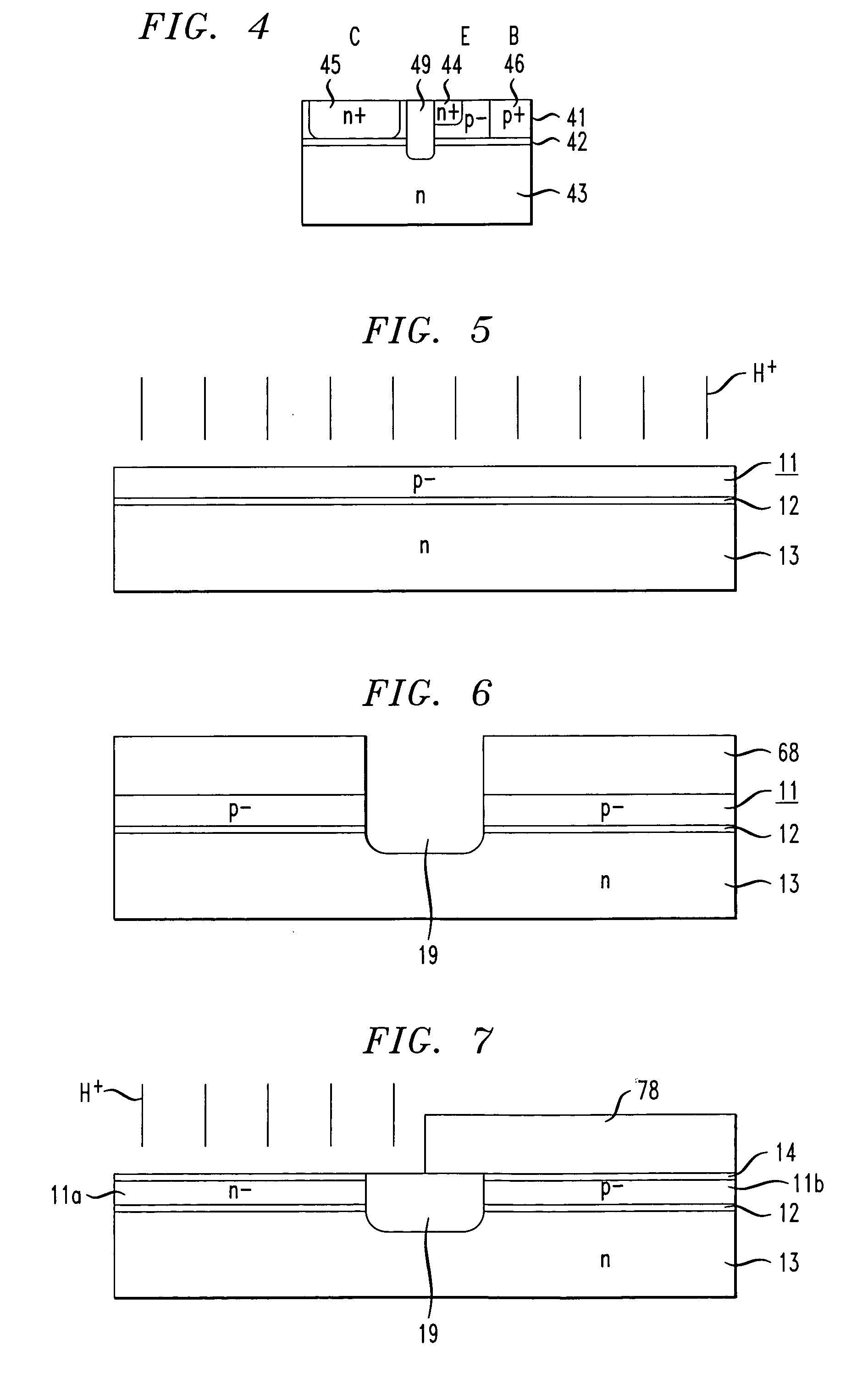
[0018] An n-type silicon wafer having an original bulk spreading resistivity of about 40 ohm-cm was implanted with 180 keV protons to a dose of about 3×10¹⁶ protons / cm2 and annealed in a nitrogen-hydrogen atmosphere at 900 degrees C. for 10 seconds to develop a buried hydrogen bubble or platelet layer, as further described in the Li patents. The implanted wafer was annealed by heating to 1180 degrees C. for 20 minutes for conversion of the top surface layer from n-type to p-type conductivity as further described in the 1996 MRS article. The surface of the annealed wafer was subjected to plasma etching to reduce the thickness of the top surface layer overlying the buried layer to approximately 0.1 μm. Other suitable means for thickness reduction include chemical etching and chemical-mechanical polishing (CMP).

[0019] For the resulting structure, FIG. 1 shows spreading resistivity versus depth as measured from the surface of the reduced-thickness surface layer. As compared with the sp...


PUM


Abstract

Semiconductor devices have device regions in which semiconductor properties such as spreading resistivity and its profile are significant. In making a p-type device region on a semiconductor wafer, an initial semiconductor device region is defined by a buried region, and an initial spreading resistivity profile is developed by annealing. After annealing, semiconductor device properties can be enhanced by removing a surface sub-region of the initial device region, and can be further improved by epitaxially growing thereon a monocrystalline film as an improved channel layer for FET devices. Such properties are relevant in MOS as well as bipolar devices.

Description

[0001] This is a divisional application of application Ser. No. 09 / 800,213 filed on Mar. 6, 2001.TECHNICAL FIELD [0002] The present invention relates to semiconductor devices and, more particularly, to VLSI / ULSI fabrication of MOSFET and bipolar transistors. BACKGROUND OF THE INVENTION [0003] The need for scaling metal-oxide-semiconductor (MOS) devices down to below 0.1 μm feature size in very-large-scale integrated (VLSI) circuits has been clearly indicated in the National Technology Road Map for, Semiconductor Technology (1997 Edition), Semiconductor Industry Association, San Jose, Calif. For such circuits, silicon-on-insulator (SOI) MOS devices appear to be promising as described in SOI Technology: Materials to VLSI (2nd edition), Boston, Kluwer, 1997. Such materials are disadvantaged, however, in having a large dose of oxygen ions implanted through the top surface layer of a silicon wafer on which devices are fabricated. [0004] An alternative method for fabricating SOI materials...

Claims


Application Information

Patent Timeline
Patent Type & Authority Applications(United States)
IPC IPC(8): H01L21/8238H01L21/84H01L27/01H01L27/092
CPCH01L21/823807H01L27/092H01L21/84
Inventor COLEMAN, JOHN HOWARD
Owner BIOTA
Why Eureka
Try Eureka