
ESD unit protection cell for distributed amplifiers

a technology of distributed amplifiers and protection cells, applied in emergency protective circuit arrangements, emergency protective arrangements for limiting excess voltage/current, emergency protective arrangements, etc., can solve problems such as device failure, large voltage waveform, and damage to transistor junctions, and achieve low voltage gain, reduce leakage current, and small size of trigger capacitors

Active Publication Date: 2007-03-29
RGT UNIV OF CALIFORNIA
View PDF21 Cites 8 Cited by
  • Summary
  • Abstract
  • Description
  • Claims
  • Application Information

AI Technical Summary

Benefits of technology

[0018] The overload protection circuit preferably has less parasitic capacitance than a conventional diode string approach for an overload protection circuit. From simulation, conventional circuits have been shown to have twice the parasitic capacitance as the overload protection circuit provided herein with similar overload protection performance. Further, the overload protection circuit of the present invention occupies one forth of the area and has one half the capacitance of a conventional diode string approach for an ESD protection circuit. The smaller size is due to the Darlington pair being more efficient for conducting excess current. Because of less capacitance, the overload protection circuit provided herein can enhance the circuit performance of the main circuit at higher frequency.
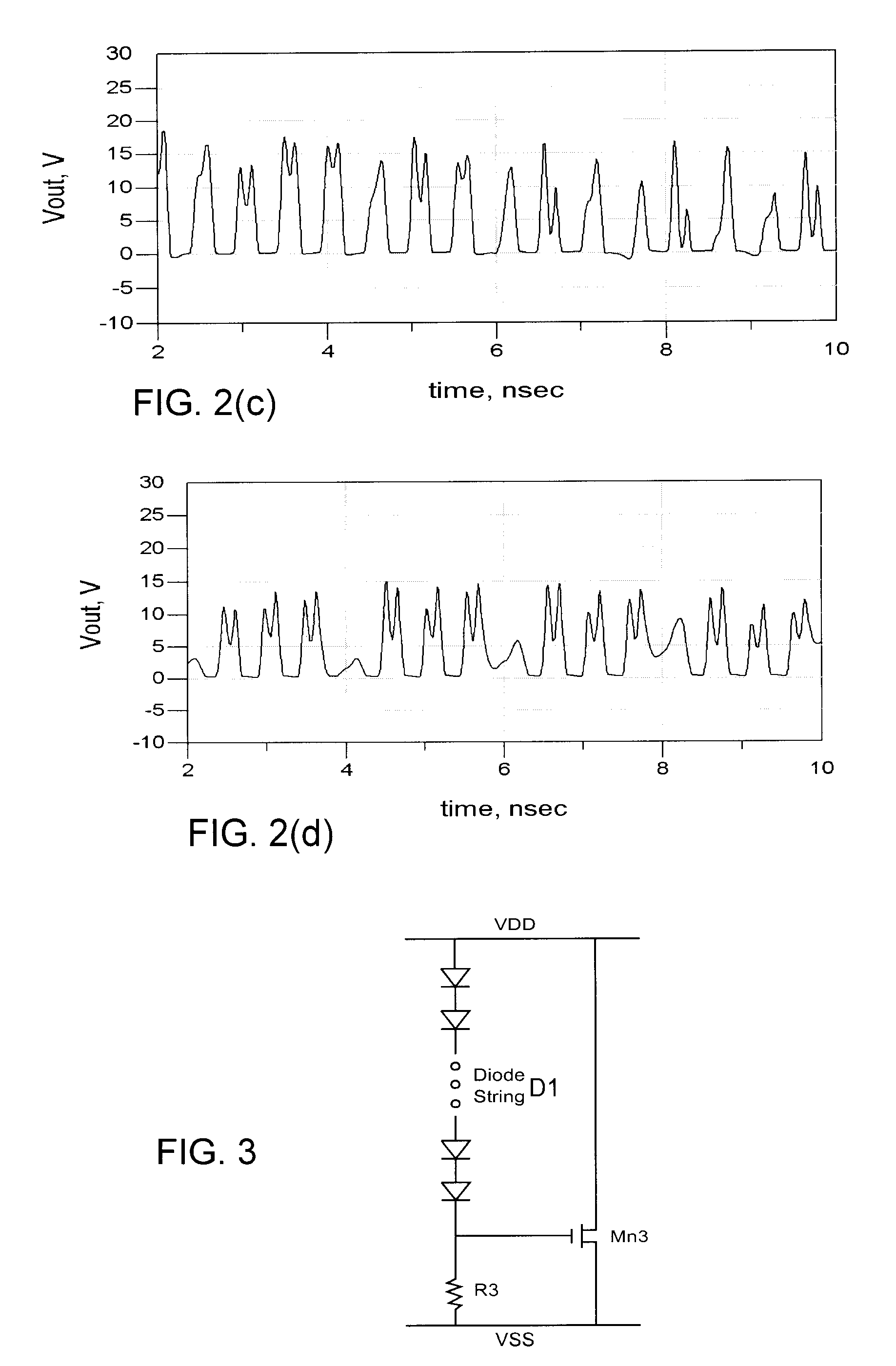
[0020] During an ESD event, ESD is coupled across the capacitor and turns on the Darlington switch. Since the Darlington switch has high current gain, only a small amount of input ESD current is needed to trigger the Darlington switch, thus resulting in a small size for the trigger capacitor. The trigger capacitor also has the benefit of blocking the DC current, reducing the leakage current at high power, improving linearly and lowering the overall capacitance loading.

Problems solved by technology

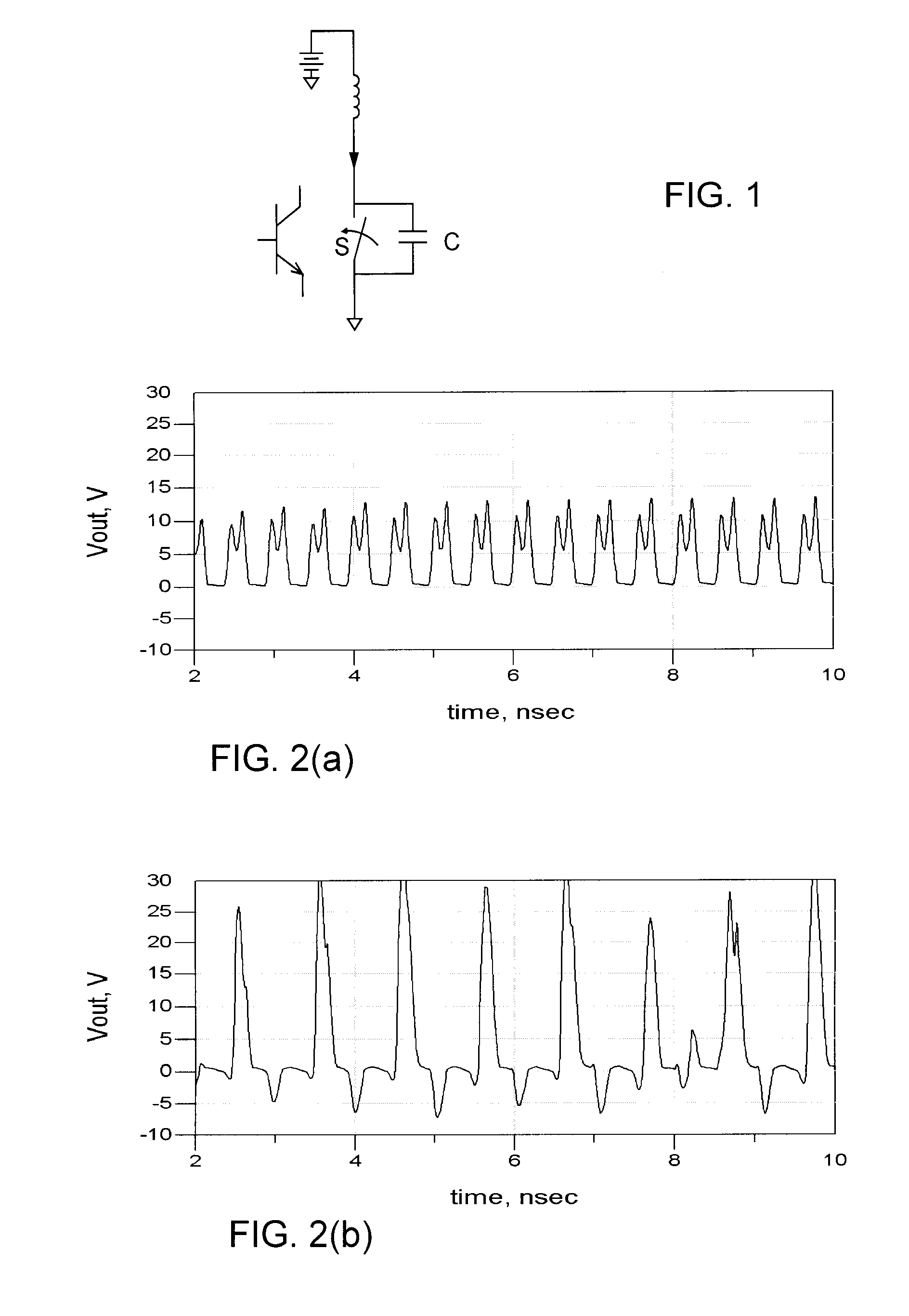
In an output impedance mismatch condition, such as in cases of a loose or obstructed antenna, the reflected signal reflects back to the transistor and produces a large voltage waveform so severe that the transistor junctions can be damaged.
Furthermore, the power amplifier, due to the requirement of delivering high output power with high efficiency, often operates at an overdrive condition in which the transistor input voltage is so high that it switches on and off the collector current.
This excessive voltage overload can lead to device failure and degradation in reliability if it is higher than the breakdown voltages.
Output impedance mismatch and modulated input signal combined with overdrive can make the voltage overload more severe.
The transient output voltage is so large that it even goes negative in which case the E-B junction is also vulnerable.
For a multiple stage amplifier, the voltage overload at the output stage can be even worse if the driver stages are overdriven, since the voltage spikes of the driver stages would be amplified by the output stages.
Usually, the transistor failures due to voltage overload occurs at the output stage, but they can also occur at the driver stages.
Because of the series resistance of the diodes, the required area of the diodes is huge.
This, in turn, increases the diode capacitance, which can limit the frequency bandwidth.
This results in declining incremental voltage drop across the diode string.
ESD protection of an RF input pin of integrated circuits, such as a telecom integrated, circuit can be difficult.
Because of this inherent problem, the base-emitter always has to endure some amount of ESD stress before the protection circuit turns on.
For this reason, ESD voltage protection for the RF input pin is more difficult.
However, since a two-diode string has a low turn on voltage due to a lower number of diodes, its leakage current is greater if the input voltage swing is large.

Method used


Image

  • ESD unit protection cell for distributed amplifiers
  • ESD unit protection cell for distributed amplifiers
  • ESD unit protection cell for distributed amplifiers

Examples


Embodiment Construction

[0044] Each of the additional features and teachings disclosed below may be utilized separately or in conjunction with other features and teachings to provide ESD protection circuits for use as on-chip voltage overload protection circuits for power amplifiers, on-chip ESD protection circuits for RF input pins for integrated circuits such as telecom integrated circuits, and unit protection cells for integration with artificial transmission lines of distributed amplifiers. Representative examples of the present invention, which examples utilize many of these additional features and teachings both separately and in combination, will now be described in further detail with reference to the attached drawings. This detailed description is merely intended to teach a person of skill in the art further details for practicing preferred aspects of the present teachings and is not intended to limit the scope of the invention. Therefore, combinations of features and steps disclosed in the follow...


PUM


Abstract

Improved protection circuits are provided for use as voltage overload protection circuits, ESD protection circuits for RF input pins, and unit protection cells for distributed amplifiers. Preferably, the protection circuits include a positive threshold voltage trigger used to trigger a switch wherein the trigger includes a diode string in series with a resistor and the switch includes a bipolar transistor switch in series with a single reverse diode. Alternatively, the trigger includes a diode string in series with a single diode and a single resistor, and is used to trigger a Darlington pair transistor switch in series with a single reverse diode. In another embodiment, a Darlington pair transistor switch is triggered by a capacitor. In use with distributive amplifiers, the ESD protection circuits are preferably absorbed inside the artificial transmission lines of the distributed amplifier.

Description

CROSS-REFERENCE TO RELATED APPLICATIONS [0001] This application claims the benefit of U.S. Provisional Application No. 60 / 718,965 filed Sep. 19, 2005, U.S. Provisional Application No. 60 / 718,967, filed Sep. 19, 2005, and U.S. Provisional Application No. 60 / 718,966 filed Sep. 19, 2005, which applications are incorporated herein by reference.FIELD OF THE INVENTION [0002] The present disclosure relates to low capacitance loading electrostatic discharge (ESD) protection circuits and, more particularly, to ESD protection circuits for use as unit protection cells for integration with artificial transmission lines of distributed amplifiers. BACKGROUND [0003] The collector output of an RF power amplifier is usually connected with a RF inductor, often referred to as the RF choke, and an output impedance matching network. The other side of the output impedance matching network is terminated with a termination, such as an antenna. The voltage at the transistor collector output is described by ...

Claims


Application Information

Patent Timeline
IPC IPC(8): H02H9/00
CPCH01L27/0255H03F1/52H03F2200/444H03F3/605H03F3/3435
Inventor MA, YINTATLI, GUANN-PYNG
Owner RGT UNIV OF CALIFORNIA
Learn More