
Nanostructured titanium monoboride monolithic material and associated methods

a monolithic material and nanostructure technology, applied in the field of hard ceramic materials, can solve the problems of high manufacturing cost, high manufacturing cost, and low availability of borides, and achieve the effects of high strength, high manufacturing cost, and high manufacturing efficiency

Inactive Publication Date: 2007-01-25
UNIV OF UTAH RES FOUND
View PDF66 Cites 6 Cited by
  • Summary
  • Abstract
  • Description
  • Claims
  • Application Information

AI Technical Summary

Benefits of technology

[0008] It would therefore be advantageous to develop improved materials and methods which produce a titanium and boron containing monolithic material having significantly increased strength, machinability, and ease of manufacture. The present invention provides methods and materials which produce nanostructured high strength titanium monoboride monolithic material which satisfies many of the above criteria.
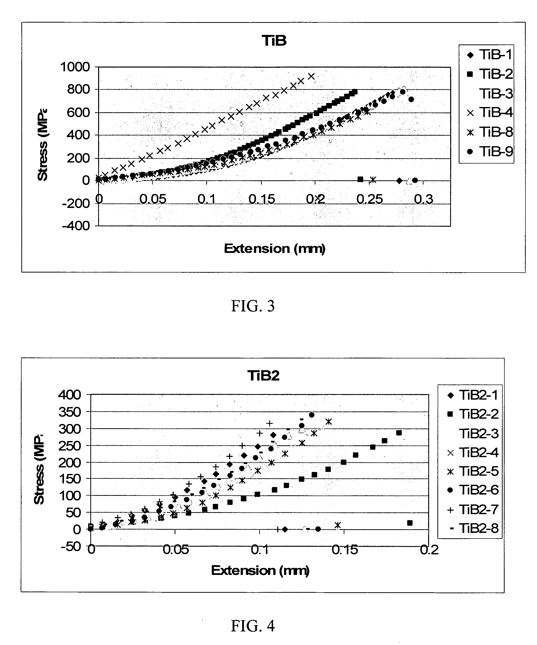
[0010] The titanium boride (TiB) material of the present invention has about three times the flexural bend strength compared to commercially available titanium diboride (TiB2) ceramic material. This is quite unusual and highly desired in hard material applications for wear and erosion resistance as well as for electrodes in metal refining. There are only a few other ceramics with this high level of strength. In addition, the titanium monoboride material of the present invention can be machined by electrical discharge machining which allows for economical formation into a wide variety of shapes.
[0012] In one aspect of the present invention, a titanium monoboride article can include titanium monoboride whiskers which are present at a volume content greater than about 80%. Further, the titanium monoboride article can also be substantially free of titanium diboride. The nanostructured titanium monoboride articles of the present invention can be readily machined using electrical discharge machining due to electrical conductivity of titanium monoboride.

Problems solved by technology

Other borides are not widely available due to difficulties in making pure and dense materials, as well as attendant high manufacturing costs.
The higher temperatures and pressures involved make this material quite expensive.
Hence, use of this material has been limited to specialized and value-added markets.
Additionally, the high cost of making titanium diboride, as well as difficulties in obtaining fully densified titanium diboride limits its flexural strength to about 300 MPa and its use to applications where there is no viable alternative.
However, typically, such materials also have substantial amounts of residual titanium metal and titanium diboride which significantly reduces the strength of the titanium monoboride material.
However, silicon nitride is not electrically conductive, which means making of complex shapes and profiles is to be done by diamond-based machining which is complicated and expensive.
Achieving full density is cumbersome, requiring even higher temperatures, pressures, and process times. Additional problems are more coarse grains and non-uniform grain structure which are some of the causes of relatively low strength (<300 MPa) titanium diboride.
The high temperatures and pressures required significantly increase the costs of manufacture.

Method used


Image

  • Nanostructured titanium monoboride monolithic material and associated methods
  • Nanostructured titanium monoboride monolithic material and associated methods
  • Nanostructured titanium monoboride monolithic material and associated methods

Examples


example 1

[0056] Preparation

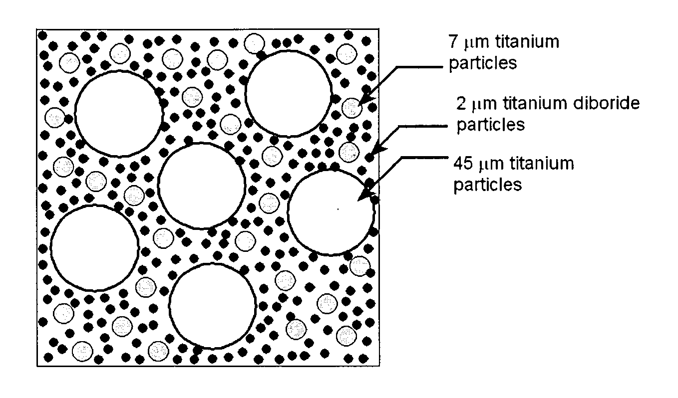
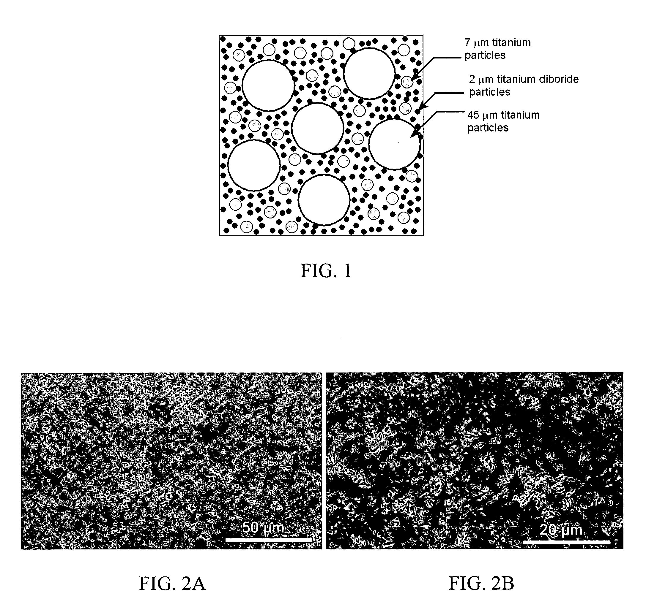
[0057] A nanostructured titanium monoboride was manufactured by carefully controlled reaction sintering of a tri-modal distribution of Ti and TiB2 powders. The relative powder sizes were important in obtaining the desired nanostructure in the final TiB material. A bi-modal titanium powder mixture having an average size of 45 μm and 7 μm and a composition of (wt. %) 0.23 O, 0.02 N, 0.01 C, 0.04 Fe, and 0.024H and titanium diboride powders having an average size of 2 μm and a composition of (wt. %) 30.3 B, 0.67 Zr, 0.01 C, 0.04 Fe, and 0.024H were provided. The titanium powder and titanium diboride powders were mixed together at 49 wt % Ti (41±2 wt % of 45 μm size and 9±1 wt % of 7 μm size powder) and 51 wt % TiB2. The powders were then thoroughly blended for 24 hours in a rotary blender with steel balls to ensure homogeneity of the mixture. These powders have a size ratio of 45:7:2, and a packing density of about 90% in the blended state, which was found to be impo...


PUM

PropertyMeasurementUnit
lengthaaaaaaaaaa
temperatureaaaaaaaaaa
particle sizeaaaaaaaaaa

Abstract

A nanostructured monolithic titanium boride (TiB) material and methods of forming such a material are disclosed and described. This material has a room-temperature four-point flexural strength about three times that of commercially available titanium diboride (TiB2). The achievement of nanostructured internal microstructural arrangement having a network of interconnected titanium monoboride whiskers affords a very high strength to this material above some of the best ceramic materials available in the market. The material contains a small amount of titanium, but it is largely made of TiB phase with substantially no TiB2. The nanostructured monolithic titanium boride material can be formed by high temperature processing of a powder precursor having carefully selected weight and size distributions of titanium and titanium diboride powders. Potential applications of this material can include wear resistant components such as die inserts for extrusion dies, nozzles, armor, electrodes for metal refining etc. An important advantage of TiB over other hard ceramics is that TiB can be cut by electro-discharge machining (EDM) without difficulty, unlike most ceramics.

Description

RELATED APPLICATIONS [0001] This application claims priority to U.S. Provisional Patent Application 60 / 680,220, filed May 10, 2005, which is incorporated herein by reference in its entirety.FIELD OF THE INVENTION [0002] The present invention relates generally to hard ceramic materials such as metal borides for wear and erosion resistant applications. More particularly, the present invention relates to monolithic nanostructured titanium boride material having much higher strength levels compared to most other hard ceramic materials and other borides. BACKGROUND OF THE INVENTION [0003] Hard ceramic materials such as oxides, carbides, nitrides and borides are engineered materials having high melting or decomposition temperature, high hardness, strength and wear resistance and resistance to high temperature oxidation and degradation as well as resistance to corrosive chemicals such as acids and bases. These ceramic materials have found applications in tools, dies, grinding media, heatin...

Claims


Application Information

Patent Timeline
Patent Type & Authority Applications(United States)
IPC IPC(8): H01B1/12
CPCC04B35/58071C04B35/581C04B35/645C04B2235/3813C04B2235/5276C04B2235/5296C30B29/605C04B2235/5463C04B2235/549C04B2235/96C30B25/005C30B29/10C04B2235/5436
Inventor CHANDRAN, K.S.
Owner UNIV OF UTAH RES FOUND
Learn More