Method and apparatus for improved clock preamplifier with low jitter

a clock signal and preamplifier technology, applied in the field of hardware implementation of clock synchronization circuits, can solve the problems of jitter being recognized as a fundamentally limiting factor of the accuracy of a signal processing sequence, noise contribution, system performance limitation, etc., and achieves little added timing jitter and rapid waveform transitions

Active Publication Date: 2006-11-16
TEXAS INSTR INC
View PDF3 Cites 7 Cited by
  • Summary
  • Abstract
  • Description
  • Claims
  • Application Information

AI Technical Summary

Benefits of technology

[0022] The invention solves the preamplifier jitter problem by making use of a bipolar complementary circuit wherein two differential pairs are constantly active and driven out of phase. The required phase splitter circuitry is implemented with a low-noise all-passive RC network which shifts and reverts the phases as needed. To prevent saturation of the active devices, a basic diode clamp network limits the swing on the collectors around the trip point of the cascaded inverter trailing the preamplifier, still allowing for the ensuing regenerative CMOS inversion out of the clamped voltage swing.
[0023] Embodiments of the present invention achieve technical advantages as a clock-signal preamplifier that converts a sinusoidal reference waveform into a rectangular waveform with very rapid waveform transitions. Advantages of embodiments of the present invention include a clock-signal preamplifier with very little added timing jitter above that contributed by the input reference waveform.

Problems solved by technology

As the role of digital logic becomes more pervasive in numerous signal-processing applications, and as the conversion of signals to digital format occurs earlier in the signal processing chain to reduce system cost and size, system performance in numerous applications such as cellular telephony and high-performance television receivers is limited by clock signal timing jitter.
Clock signal timing jitter is now generally recognized as a fundamentally limiting factor of the accuracy of a signal processing sequence.
The noise contribution due to the uncertainty of the sampling instant of a high frequency input signal is directly affected by timing jitter in both the clock source and the clock distribution network.
The transition speed of the output voltage of this circuit at the transition times of the rectangular waveform, which is related to its output timing jitter, is limited by the passive pull-up arrangement of the resistors R1 and R4 and parasitic circuit capacitance, and these circuit elements contribute to limiting the ultimate timing performance of the circuit due to the limited slope of the voltage transitions.
Although the gain of this circuit is higher than the gain of the circuit illustrated in FIG. 2A, its noise is also higher, resulting in little or no improvement in its timing jitter.
Nonetheless, MOSFETs 242 and 244 provide limited switching speed at the pull-down transitions of the rectangular waveform outputs, which still limits the timing jitter that can be produced by such a circuit.
In particular, at lower sampling frequencies the inherent hysteresis built into the circuit adversely impacts the jitter performance of this solution, making it worse than the aforementioned prior art for rates of 30MS / s or lower in the present technology.
The main limitations of the prior art circuits are thus passive pull-up of the output, which results in slow transition times, making them more sensitive to timing uncertainties, and forced usage of MOSFET devices to yield larger output swings, which generally results in reduced output voltage transition slopes and higher device noise (e.g., a 1 / f-dependent noise component), in turn requiring additional buffer stages which introduce more sources of jitter, as described by A. Zanchi, et al., in “A 16-Bit 65 MS / s 3.3 V Pipeline ADC Core in SiGe BiCMOS with 78-dB SNR and 180 fs Jitter”, cited above, and by J. A. McNeill, “Jitter in Ring Oscillators,” published in the IEEE Journal of Solid-State Circuits, Vol. 32, No. 6, June 1997, on pages 870-879.
Despite the advances in clock-signal preamplifiers, a remaining obstacle to obtaining low timing jitter in the conversion of a sinusoidal timing reference signal to an amplified and rectangular waveform signal is the need to increase the slope of the output voltage waveform at its voltage transition points so that the preamplifier introduces less timing signal jitter in the generation of a rectangular output waveform.

Method used


Image

  • Method and apparatus for improved clock preamplifier with low jitter
  • Method and apparatus for improved clock preamplifier with low jitter
  • Method and apparatus for improved clock preamplifier with low jitter

Examples


Embodiment Construction

[0040] The making and using of the presently preferred embodiments are discussed in detail below. It should be appreciated, however, that the present invention provides many applicable inventive concepts that can be embodied in a wide variety of specific contexts. The specific embodiments discussed are merely illustrative of specific ways to make and use the invention, and do not limit the scope of the invention.

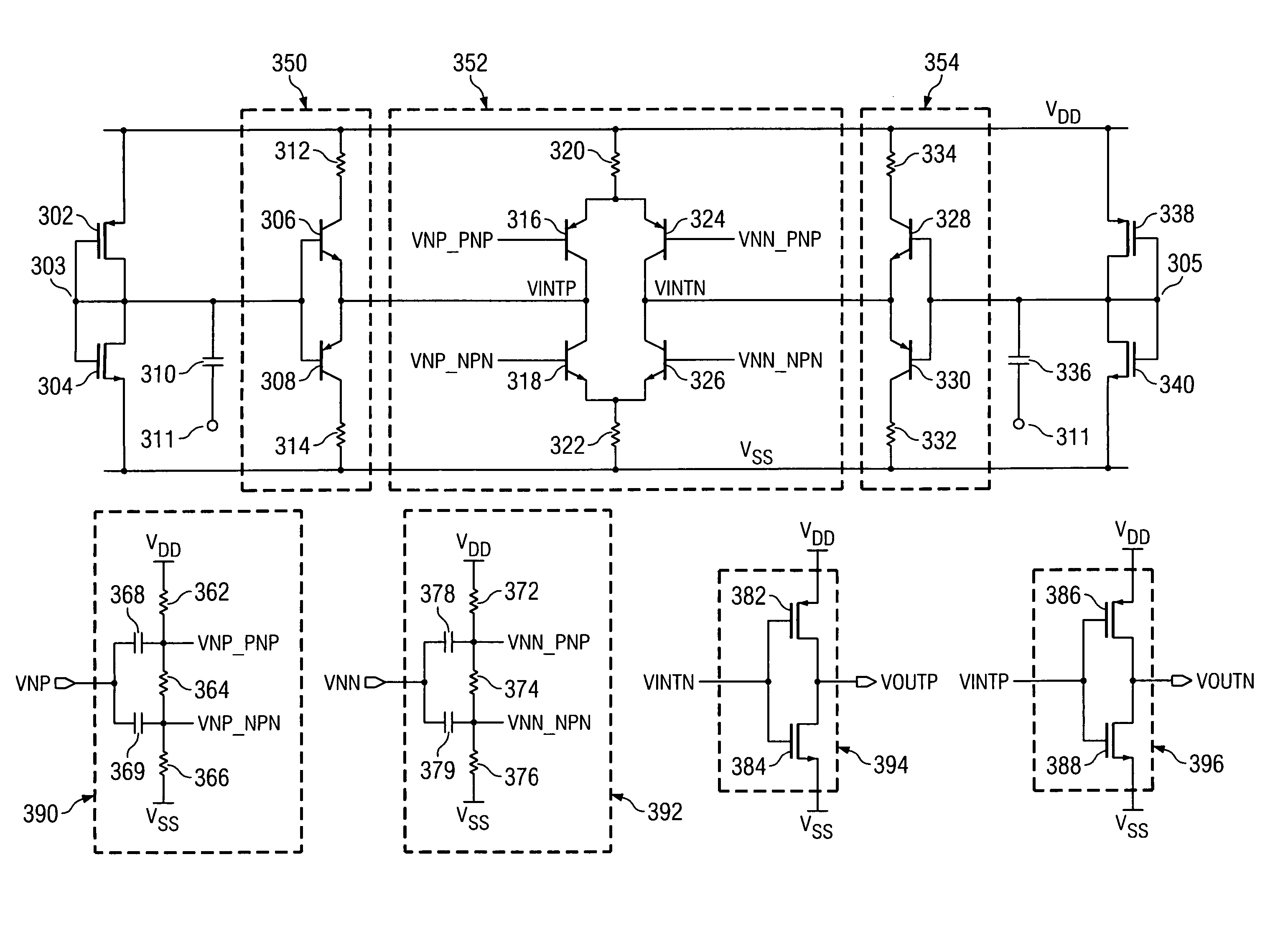
[0041] Embodiments of the present invention will be described with respect to preferred embodiments in a specific context, namely a clock signal preamplifier comprising two complementary pairs of differentially coupled transistors, coupled in series between the circuit nodes of a bias voltage source, that produces a rectangular output waveform with very fast voltage transitions from a sinusoidal input voltage, and with very little timing jitter. The clock signal preamplifier preferably comprises bipolar devices and includes diode dampers comprising a totem-pole arrangement ...


PUM


Abstract

A clock signal preamplifier comprises complementary pairs of differentially coupled transistors, with an output signal coupled to an inverter further comprising a totem-pole arrangement of complementary MOSFET transistors. The input signal to the preamplifier is typically sinusoidal, and the output signal is rectangular. Preferably, the differentially coupled transistors are bipolar, and a pair of diode damper circuits with bipolar transistors is preferably coupled to the complementary pairs of differentially coupled transistors. A reference voltage source is coupled to the control terminals of the damper transistors. A reference voltage source, which preferably comprises a totem-pole arrangement of complementary MOSFET transistors with its output node is coupled to its input node, provides a reference voltage for the diode damper circuits. Preferably, MOSFET transistors of the reference voltage source and MOSFET transistors of like kind of the inverter are configured to have substantially identical threshold voltages.

Description

TECHNICAL FIELD [0001] This invention relates generally to hardware implementations of clock synchronization circuits, and in particular, to a method and implementation of digital clock synchronization circuits for analog-to-digital conversion comprising an integrated circuit. BACKGROUND [0002] An essential element of design in digital systems that broadly affects system performance is the creation and distribution of a precise clock signal to serve as a stable timing reference for synchronizing digital logic, particularly for sampling analog signals prior to their conversion to a digital form or for converting digital signals back to an analog form. As the role of digital logic becomes more pervasive in numerous signal-processing applications, and as the conversion of signals to digital format occurs earlier in the signal processing chain to reduce system cost and size, system performance in numerous applications such as cellular telephony and high-performance television receivers ...

Claims


Application Information

Patent Timeline
IPC IPC(8): H03F3/16
CPCH03F3/42H03F3/4517H03F3/4508
Inventor ZANCHI, ALFIOCORSI, MARCO
Owner TEXAS INSTR INC
Why Eureka
Try Eureka