Memory device having components for transmitting and receiving signals synchronously

a memory device and synchronous transmission technology, applied in the direction of information storage, static storage, digital storage, etc., can solve the problems of high error-prone internal data transfer and vice versa low bit rate in the inpuvoutput section, and increase the risk of error with the factor of conversion, so as to improve the exchange of signals between the interfaces of the components or sections of the memory device, the effect of improving the security, stable and reliabl

Inactive Publication Date: 2006-08-17
POLARIS INNOVATIONS
View PDF2 Cites 4 Cited by
  • Summary
  • Abstract
  • Description
  • Claims
  • Application Information

AI Technical Summary

Benefits of technology

[0009] One aspect of the present invention provides an improved memory device and more particularly, a memory device operable at high external and low internal bit rates with no or a low risk of errors.
[0016] Embodiments of the present invention provide the advantage that the exchange of signals between the interfaces of the components or sections of the memory device is improved and made more secure. Particularly advantages are achieved because the input / output section of the memory device converts an external lowly parallel high bit rate data transfer to an internal highly parallel low bit rate data transfer and vice versa. This conversion is particularly stable and reliable when components or sections of the memory device or their interfaces are synchronised by a clock signal which is derived from an external clock signal by clock division. In this case, the external clock is divided by the same factor as the bit rate is reduced from external to internal and the number of parallel lines is increased correspondingly from external to internal.

Problems solved by technology

On the other hand, due to the constraints of the semiconductor technology used for the production of memory devices, the bit rates on internal lines of memory devices will be much lower and rise much slower than the external bit rates.
The conversion of lowly parallel (i.e., relatively few parallel lines; e.g., eight or less parallel lines) high bit rate external data transfer to highly parallel (i.e., relatively high number of parallel lines; e.g., sixty four or more parallel lines) low bit rate internal data transfer and vice versa in the inpuVoutput section is highly error-prone.
The risk of an error increases with the factor of conversion.

Method used


Image

  • Memory device having components for transmitting and receiving signals synchronously
  • Memory device having components for transmitting and receiving signals synchronously
  • Memory device having components for transmitting and receiving signals synchronously

Examples


first embodiment

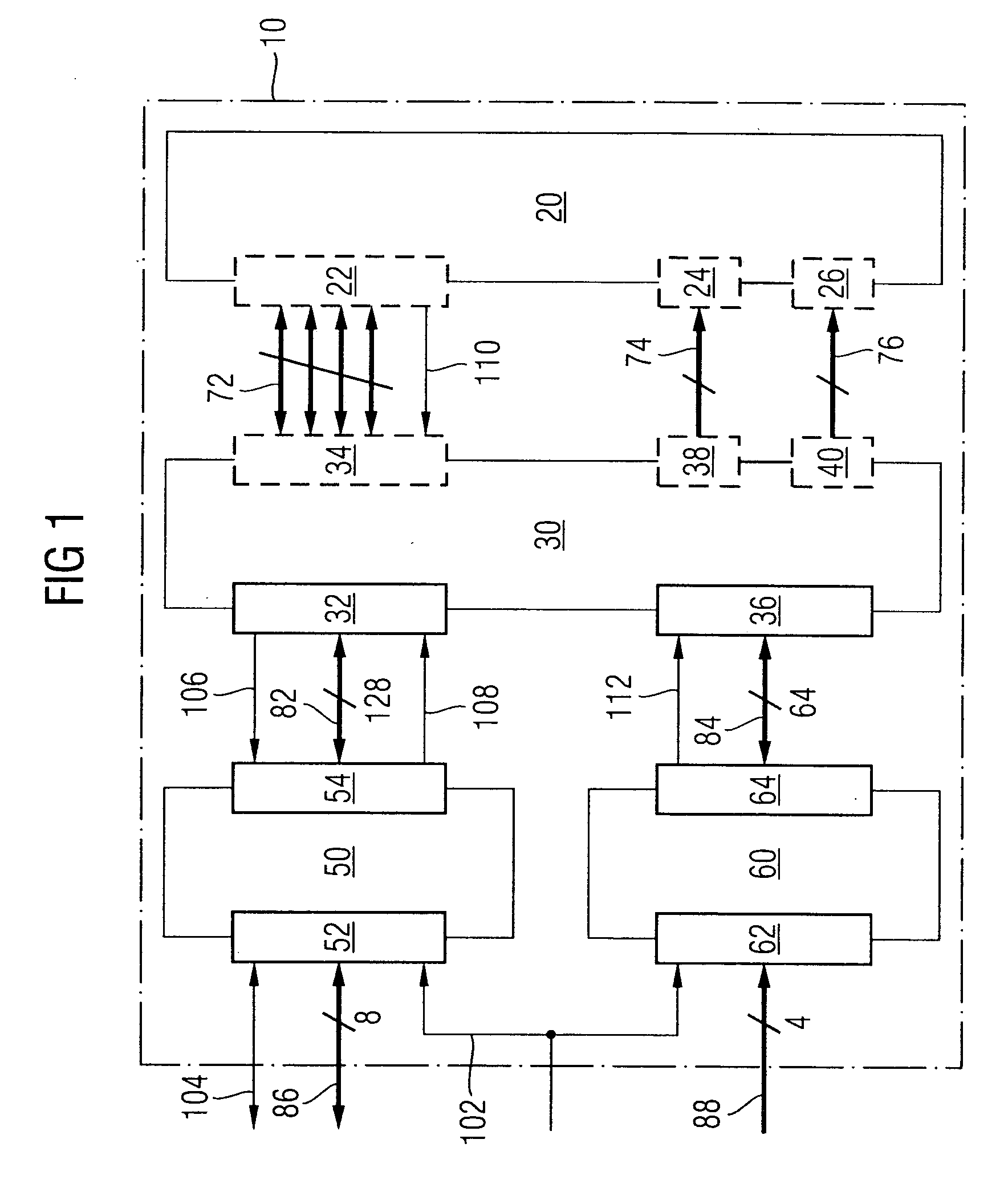
[0024]FIG. 1 is a schematic circuit diagram of a memory device 10 according to the present invention. The memory device 10 comprises an array 20 of memory cells. The memory cells may be dynamic memory cells, and each cell may include a storage capacitor and an access transistor connecting the storage capacitor to a bit line, the access transistor being controlled via a word line. Alternatively, the memory cells of the array 20 may be any other kind of dynamic or static memory cells.

[0025] The array 20 of memory cells is provided with a first interface 22 for receiving data, or data signals, to be stored in the memory cells of the array 20 and for transmitting data, or data signals, read from memory cells of the array 20. Further, the array 20 is provided with second and third interfaces 24, 26 for receiving addresses, or address signals, of memory cells in which data are to be stored or from which data are to be read. In one embodiment, the second interface 24 receives a column addr...

second embodiment

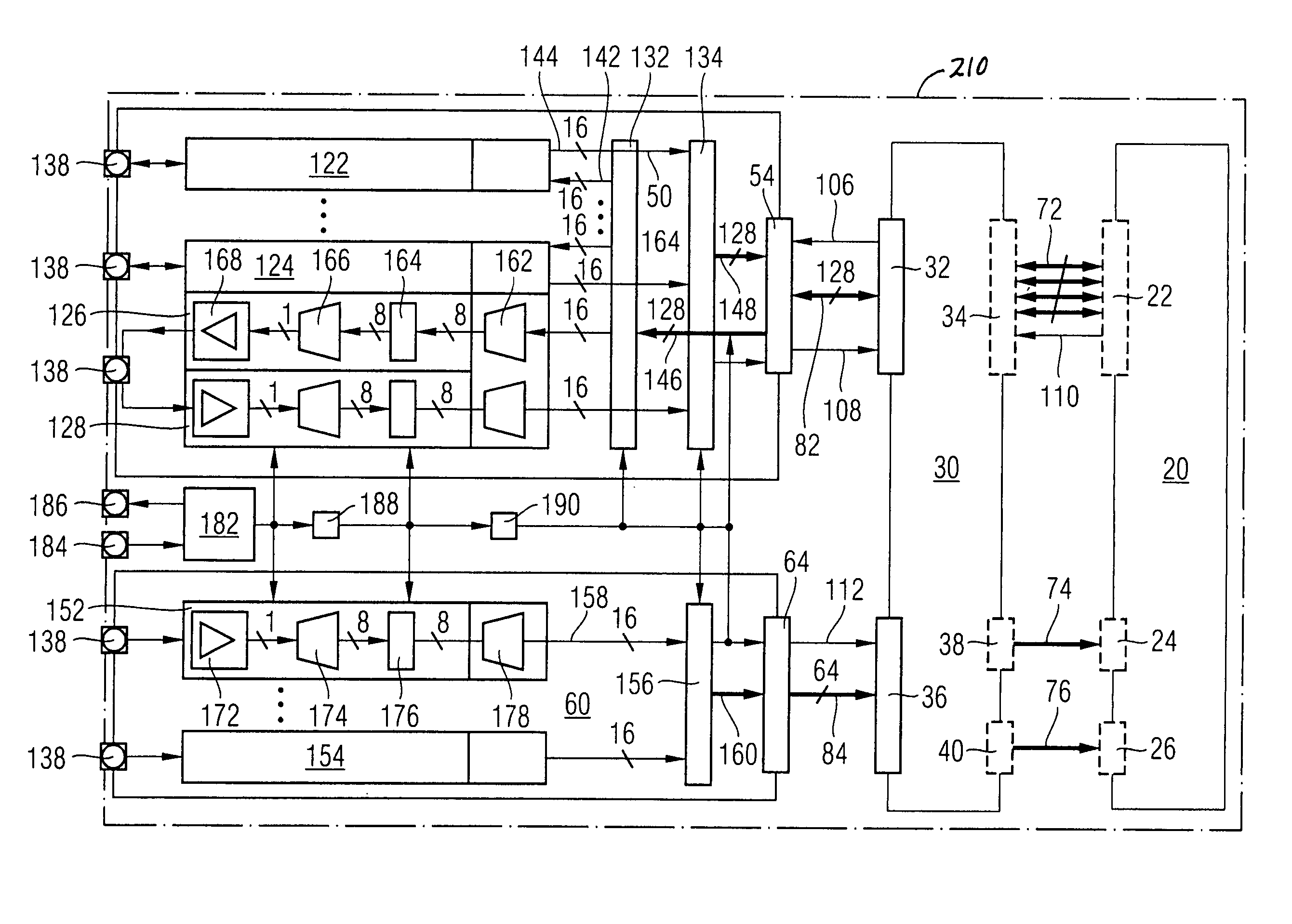
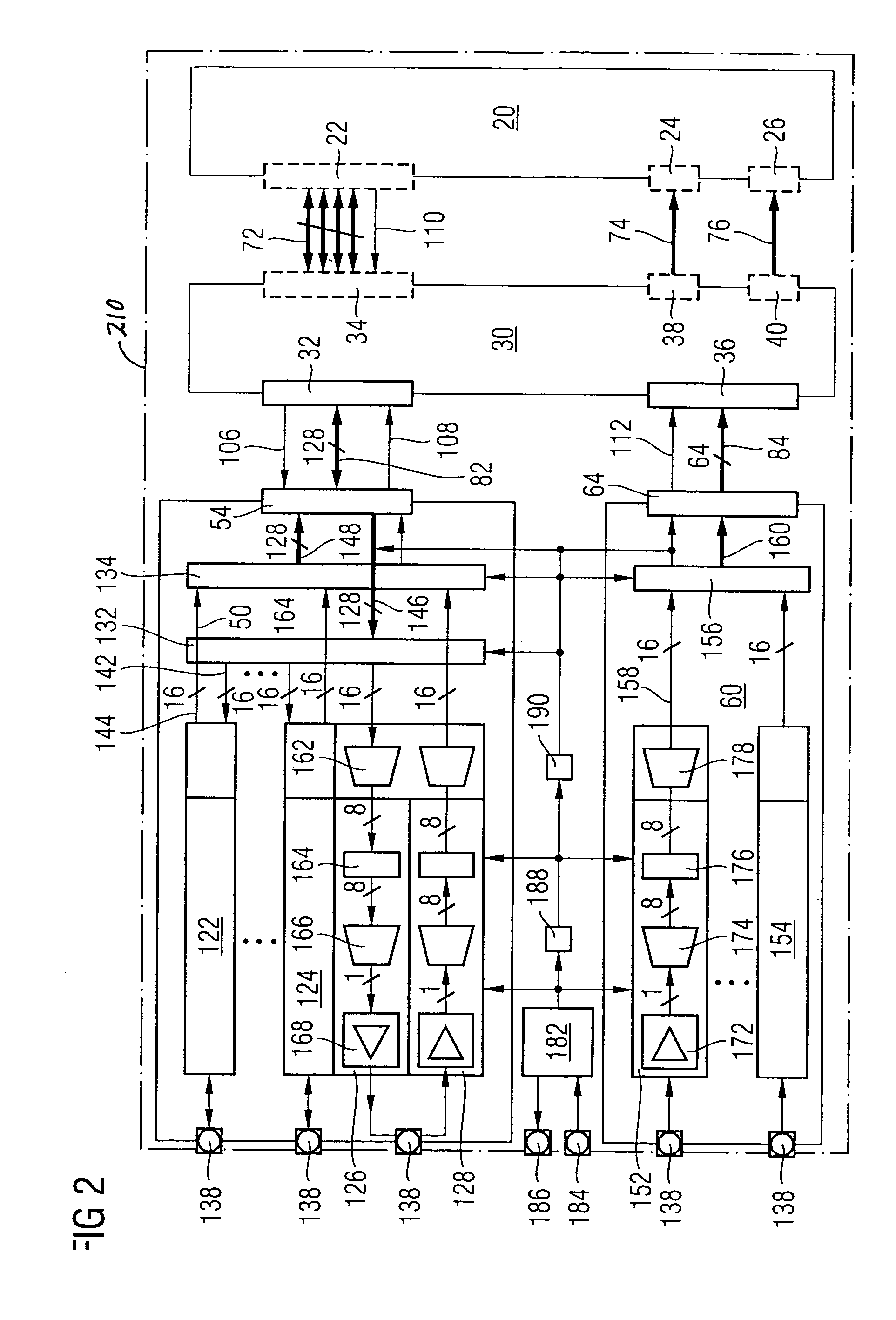
[0045]FIG. 2 is a schematic circuit diagram of a memory device 210 according to the present invention. This memory device 210 is similar to the memory device 10 described above with reference to FIG. 1. In contrast to FIG. 1, the internal configuration of the input / output section 50, 60 is displayed.

[0046] The first part 50 of the input / output section comprises eight lanes with identical inner structure. Two of the lanes, the first lane 122 and the seventh lane 124, are displayed merely as rectangles. As shown in detail with regard to the eighth lane, it is displayed that each lane consists of a transmitting circuit 126 and a receiving circuit 128.

[0047] Furthermore, the first part 50 of the input / output section comprises a first FIFO memory 132 and a second FIFO memory 134. The first part 50 of the input / output section further comprises eight contact pads 138. Each of the contact pads 138 is connected to one of the lanes 122, 124. From the eighth lane, it is shown that in each lan...

fourth embodiment

[0077] In the fourth embodiment, the transfer of command, address and data signals from the memory controller or any other external circuit to the second part 60 of the input / output section, from there to the control logic 30 and from the control logic 30 to the array 20 of memory cells, is controlled by clock signals which are transmitted parallel to the command, address and data signals via clock lines 102, 112, 114. The clock signal transferred via the clock line 112 from the second part 60 of the input / output section to the control logic 30 is the same as or is derived by clock division from the clock signal transferred from the memory controller to the input / output section 50, 60 via the clock line 102. The clock transferred from the control logic 30 to the array 20 of memory cells via the clock line 114 is the same as or derived by clock division from the clock transferred from the input / output section 50, 60 to the control logic 30 via the clock line 112. The whole control lo...


PUM


Abstract

One embodiment of the present invention provides a memory device comprising an array of memory cells, a control logic for writing data to and reading data from the array of memory cells, the control logic comprising a first interface, an input / output section for exchanging data, address and control signals with a circuit external to the memory device, the input / output section comprising a second interface for sending signals to and receiving signals from the first interface of the control logic, and a synchronizing facility connected to the first interface of the control logic and to the second interface of the input / output section for synchronizing the first interface of the control logic and the second interface of the input / output section.

Description

BACKGROUND OF THE INVENTION [0001] 1. Field of the Invention [0002] The present invention refers to a memory device and to memory device parts for transmitting and receiving signals in a synchronous way. [0003] 2. Description of the Related Art [0004] A conventional memory device comprises an array of memory cells, a control logic for addressing single memory cells or groups of memory cells and for writing data to and reading data from the array of memory cells and an input / output section. The memory device exchanges data, address and control signals via the input / output section with circuits external to the memory device, for example, with a memory controller. The array of memory cells, a control logic and the input / output section include interfaces for communication between them. Signal exchange between the interfaces of the array of memory cells, the control logic and the input / output section is asynchronous. [0005] The input / output section comprises receiver circuits and on-chip...

Claims


Application Information

Patent Timeline
IPC IPC(8): G11C8/00
CPCG11C7/1051G11C7/1066G11C7/1072G11C7/1078G11C7/1093
Inventor GREGORIUS, PETER
Owner POLARIS INNOVATIONS
Why Eureka
Try Eureka