Capacitor device and method of manufacturing the same

a capacitor and film thickness technology, applied in the field of capacitor devices, can solve the problems of difficult to get the dielectric layer having a uniform film thickness, miniaturization of the capacitor device, etc., and achieve the effect of reducing tolerance and responding easily

Active Publication Date: 2006-04-27
SHINKO ELECTRIC IND CO LTD
View PDF7 Cites 4 Cited by
  • Summary
  • Abstract
  • Description
  • Claims
  • Application Information

AI Technical Summary

Benefits of technology

[0026] The capacitor device of the present invention is manufactured by the above manufa

Problems solved by technology

In case the dielectric layer is formed by the roller coater, or the like, it become difficult to get the dielectric layer having a uniform film thickness when a surface of the underlying l

Method used


Image

  • Capacitor device and method of manufacturing the same
  • Capacitor device and method of manufacturing the same
  • Capacitor device and method of manufacturing the same

Examples


first embodiment

[0031]FIGS. 2A to 2M are sectional views showing a method of manufacturing a capacitor device according to a first embodiment of the present invention.

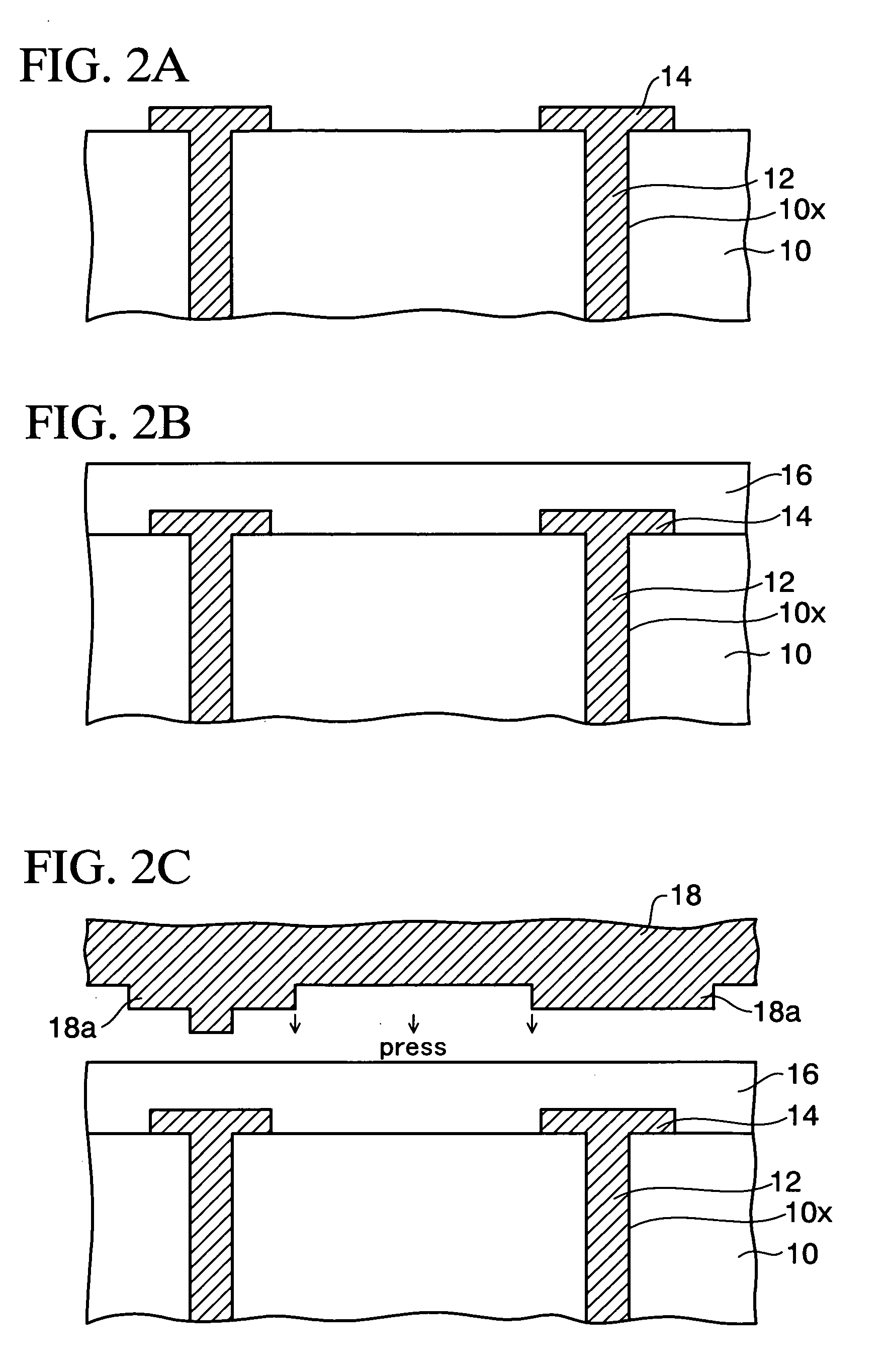
[0032] In the method of manufacturing a capacitor device in the first embodiment, as shown in FIG. 2A, first a core substrate 10 is prepared. Through holes 10x passing through the core substrate 10 are provided in the core substrate 10, and through electrodes 12 are formed in the through holes 10x. Also, first wiring layers 14 connected mutually via the through electrodes 12 are formed on both surface sides of the core substrate 10 (the lower surface side of the core substrate 10 is not illustrated).

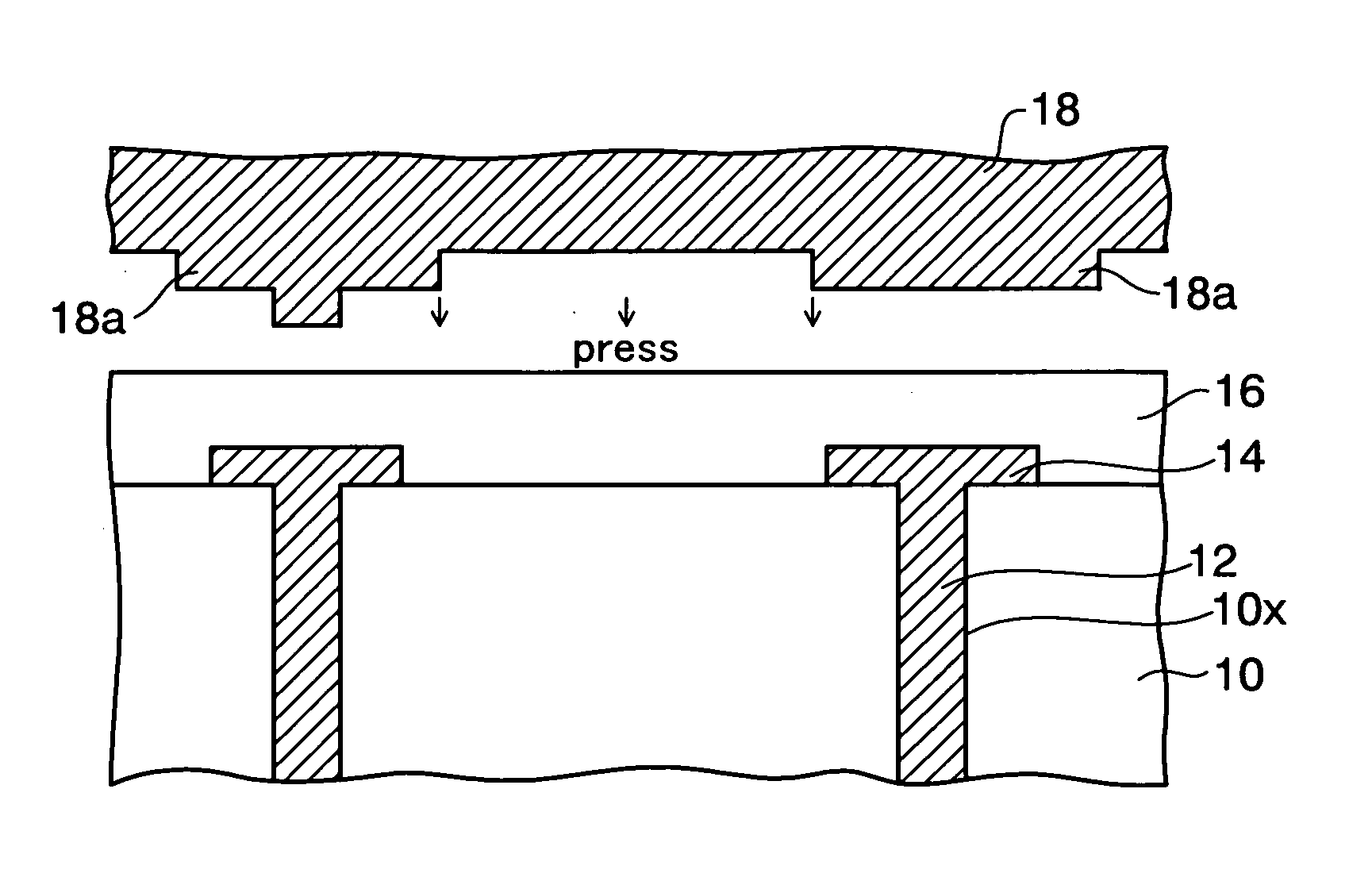
[0033] Then, as shown in FIG. 2B, a first interlayer insulating layer 16 for covering the first wiring layers 14 is formed by pasting a resin film on an upper surface of the core substrate 10. Then, as shown in FIG. 2C, a die 18 having projected portions 18a used in the imprinting process is prepared. Then, surfaces of the projected port...

second embodiment

[0053]FIGS. 3A to 3I are sectional views showing a method of manufacturing a capacitor device according to a second embodiment of the present invention. The second embodiment shows such a mode that dielectric layer patterns of the capacitors are formed to be buried in the insulating layer on the basis of the imprinting process. Detailed explanation about the same steps as those in the first embodiment will be omitted herein.

[0054] First, as shown in FIG. 3A, like FIG. 2B in the first embodiment, the core substrate 10 having the through holes 10x, the through electrodes 12 provided in the through holes 10x, and the first wiring layers 14 connected to the through electrodes 12 is prepared. Then, the first interlayer insulating layer 16 is formed on the upper surface of the core substrate 10.

[0055] Then, as shown in FIG. 3B, a contact hole 16z having a depth that reaches the first wiring layer 14 is formed by processing the first interlayer insulating layer 16 by means of the drill o...


PUM


Abstract

A method of manufacturing a capacitor device of the present invention, includes the steps of, forming an insulating layer on a substrate, forming a recess portion in the insulating layer by an imprinting process, forming a lower electrode by filling a metal layer in the recess portion in the insulating layer, forming a photosensitive dielectric layer on the lower electrode, forming an upper electrode on the dielectric layer, and forming a dielectric layer pattern under the upper electrode by exposing/developing the dielectric layer while using the upper electrode as a mask.

Description

CROSS-REFERENCE TO RELATED APPLICATIONS This application is based on and claims priority of Japanese Patent Application No. 2004-312744 filed on Oct. 27, 2004, the entire contents of which are incorporated herein by reference. BACKGROUND OF THE INVENTION [0001] 1. Field of the Invention [0002] The present invention relates to a capacitor device and a method of manufacturing the same and, more particularly, a capacitor device that is arranged on a circuit substrate and applicable to a decoupling capacitor, a high-frequency filter, and the like and a method of manufacturing the same. [0003] 2. Description of the Related Art [0004] In the prior art, there is the capacitor device that is arranged on the circuit substrate and functions as a decoupling capacitor, a high-frequency filter, or the like. In the method of manufacturing the capacitor device in the prior art, as shown in FIG. 1A, a first copper layer 102a is formed on a substrate 100, then a photosensitive dielectric layer 104a...

Claims


Application Information

Patent Timeline
IPC IPC(8): H01L29/94
CPCH01L21/76807H01L21/76838H01L23/50H01L23/5223H01L23/642H01L28/40H05K1/162H05K3/0023H05K3/005H05K3/107H05K3/4602H05K3/465H05K3/4652H05K2201/0187H05K2201/09509H05K2203/0108H05K2203/0551H05K2203/1189H01L2924/0002H01L2924/00H10B12/00
Inventor TANAKA, KOICHI
Owner SHINKO ELECTRIC IND CO LTD
Why Eureka
Try Eureka