Semiconductor device
a technology of semiconductors and devices, applied in the direction of semiconductor devices, basic electric elements, electrical appliances, etc., can solve the problems of increasing leakage current, lowering current, and extremely high threshold voltage vth of p-type mosfet and a sufficient level of electric field
- Summary
- Abstract
- Description
- Claims
- Application Information
AI Technical Summary
Benefits of technology
Problems solved by technology
Method used
Image

Examples
example 1
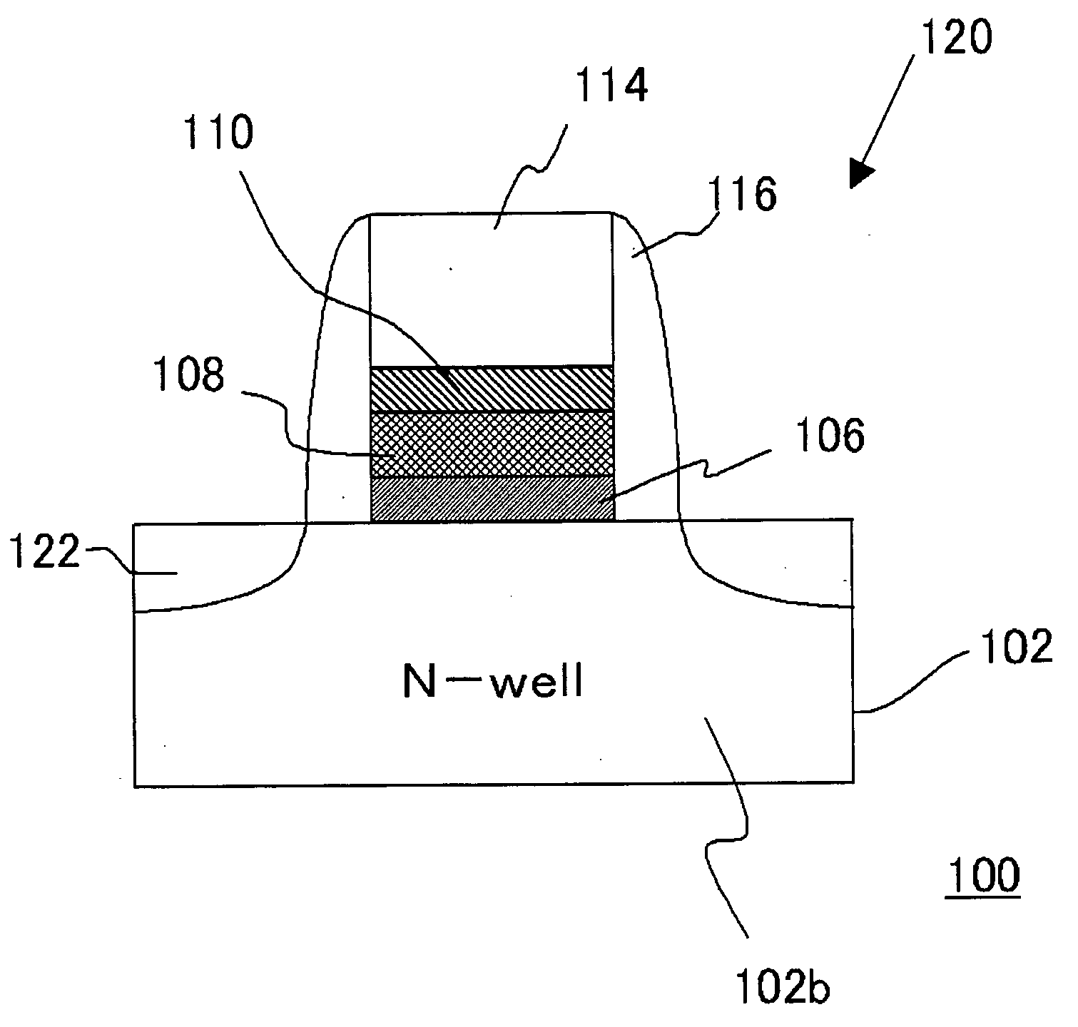
[0070] Using the P-type MOSFET 120 configured as shown in FIG. 1, investigations were made on whether (i) a SiO2 film, (ii) a SiN film and (iii) a Al2O3 film, as the blocking film disposed between the high-dielectric-constant film 108 and the polysilicon film 114, have a function of blocking diffusion of a metal composing the high-dielectric-constant film into polysilicon (referred to as “blocking function”, hereinafter), or not.
[0071] Results are shown below: [0072] (i) SiO2 film: Because this film needs a considerable increase in the thickness in order to satisfy an effective level of the blocking function, and has a low relative dielectric constant, it was found to impair the effect of reducing EOT (equivalent SiO2 thickness) attained through use of the high-dielectric-constant film as the gate insulating film; [0073] (ii) SiN film: Found to have a certain level of blocking function. The SiN film has a relative dielectric constant larger than the SiO2 film has, but is oxidized w...
example 2
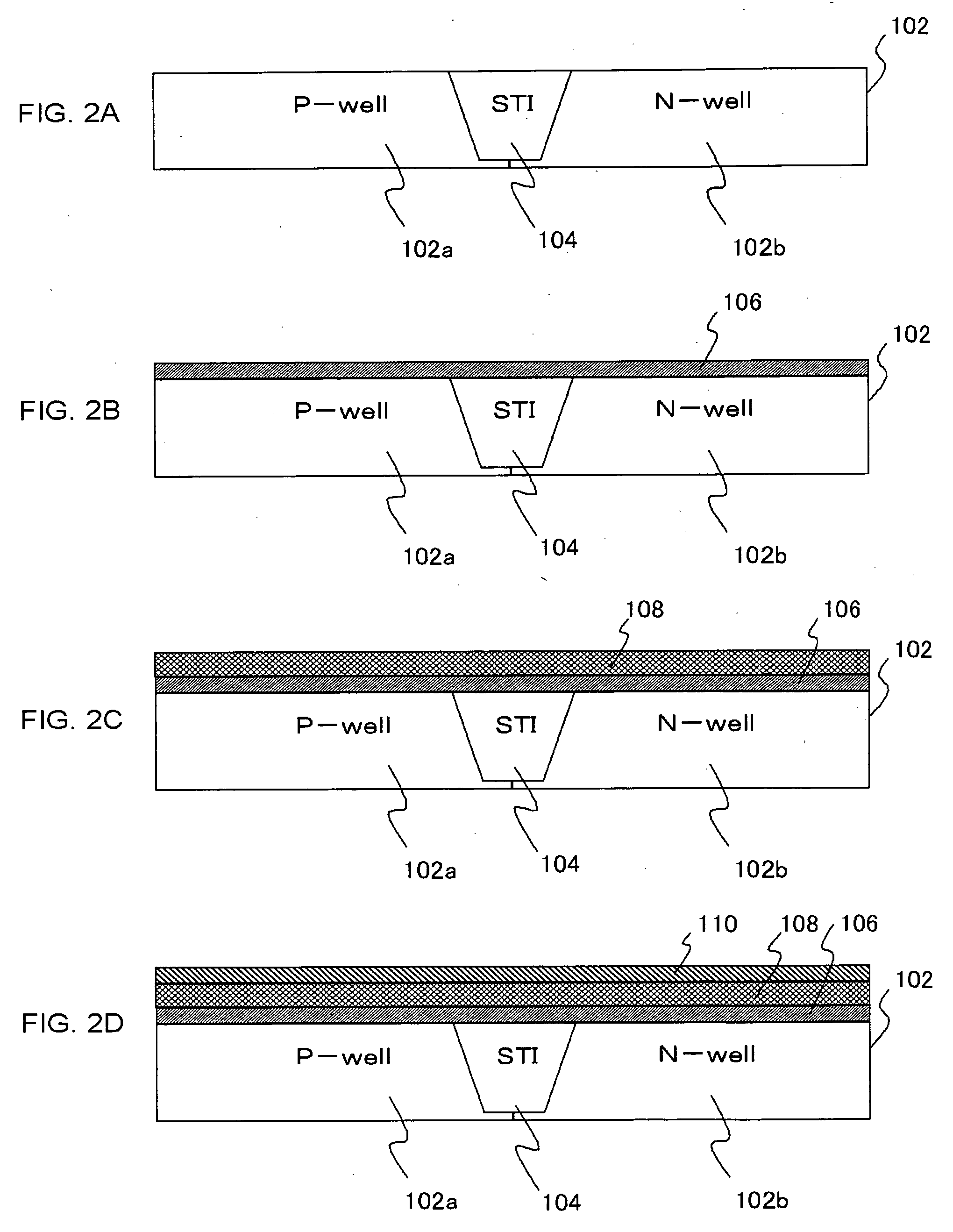
[0075] The P-type MOSFET 120 configured as shown in FIG. 1, without the sidewall insulating film 116, were fabricated.
[0076] The silicon oxide film 106, the thickness of which was about 1.0 to 2.0 nm, was formed on the silicon substrate 102. Then, the HfSiO film, the thickness of which was about 1.0 to 2.5 nm, was formed thereon by the CVD process. Subsequently, the nitrogen plasma treatment was thereafter carried out on the HfSiO film to form the HfSiON film (high-dielectric-constant film 108). Then, the Al2O3 film (blocking oxide film 110) was formed on the high-dielectric-constant film 108. The polysilicon film 114 was formed on the blocking oxide film 110, and the polysilicon film 114 was patterned to form the gate electrode. Then, ion-implant was performed to form the source and drain (impurity-diffused regions 122). Subsequently, activation was performed by annealing at about 1000° C. to form the transistor structure. Here, three transistor structures each having the Al2O3 fi...
reference example 1
Ref. 1
[0077] The silicon oxide film was formed on the silicon substrate. Then, the polysilicon film was formed on the silicon oxide film, and the polysilicon film was patterned to form the gate electrode. Then, ion-implant was performed to form the source and drain. Subsequently, activation was performed by annealing at about 1000° C. to form the transistor structure.
PUM
 Abstract
Description
Claims
Application Information
 - R&D
- Intellectual Property
- Life Sciences
- Materials
- Tech Scout
- Unparalleled Data Quality
- Higher Quality Content
- 60% Fewer Hallucinations
Browse by: Latest US Patents, China's latest patents, Technical Efficacy Thesaurus, Application Domain, Technology Topic, Popular Technical Reports.
© 2025 PatSnap. All rights reserved.Legal|Privacy policy|Modern Slavery Act Transparency Statement|Sitemap|About US| Contact US: help@patsnap.com