
Soldering method and solder joints formed therein

a solder joint and soldering method technology, applied in the direction of soldering apparatus, manufacturing tools, transportation and packaging, etc., can solve the problems of increased manufacturing process and energy cost in the electronic industry, increased cost of sn—in solder, and high cost of indium solder, etc., to achieve good wetting, good fatigue resistance, and low melting point

Inactive Publication Date: 2005-12-08
NATIONAL TSING HUA UNIVERSITY
View PDF6 Cites 17 Cited by
  • Summary
  • Abstract
  • Description
  • Claims
  • Application Information

AI Technical Summary

Benefits of technology

[0008] In addition to the abovementioned advantages, Professor Ipser of the University of Vienna, Austria has pointed out the problem that a solder with a high tin content might form a brittle tin pest at a low temperature [2004 TMS annual meeting, Charlotte, N.C., USA]. Ipser has disclosed that the problem of tin pest can be significantly improved by introducing indium into tin. This will be an advantage of the present invention which adopts an indium layer on the lead-free solder. The reasons why a lead-free solder joint having a gradient of In content of the present invention are applicable are a low melting point of indium, and a broad and mild eutectic region of the eutectic Sn—In alloy. Tamura and Murayam [JP2001219267, 2001] have developed a method for preparing a Sn—In—Bi-based solders by two plating steps (Sn—In plating and Sn—Bi plating) in 2001. However, the objective of their study is to prepare a ternary alloy, which is not related to the features of the present invention of using the low melting point of indium, and a broad and mild eutectic region of the eutectic Sn—In alloy. The use of a lead-free solder is imperative and has become a mainstream in the development of the flip chip technique. The trend of a reduced clearance has made the use of a plating technique being a must. Thus, the present invention has an immediate advantage of commercial applications.
[0009] This invention forms an indium or indium alloy layer on top of a Sn based lead-free solder. The indium or indium alloy layer can be formed by various methods, such as plating, deposition, printing, and dipping, etc. The indium-containing layer melts during the soldering process, wets the substrate in contact therewith and the lead-free solder, and forms a sound solder joint after cooling. Since the melting point of indium is 156.6° C., even lower than the melting point, 183° C., of the eutectic Sn—Pb alloy, so the soldering process can be carried out at a temperature lower than the conventional soldering process. During the soldering process, the indium reacts with the Sn based Pb-free solder alloy to form a liquid phase region. Since the eutectic temperature of Sn—In is at 120° C., the surface of the In- or In alloy-deposited Pb-free solder remains as the liquid phase and have a good wetting with the substrate during the short time of the soldering process, while an In gradient is formed in the In- or In alloy-deposited Pb-free solder.
[0010] According to the present invention, indium or indium alloy is plated on the external surface of the Pb-free solder. Indium has many advantages including low melting point, good fatigue resistance, and mild interfacial reactions, etc. More importantly, from pure In to a eutectic composition, an In—Sn system has a broad range of compositions, and a gentle gradient of the melting point and composition changes. This will enable the present invention having a wider applicable composition range for forming a concentration gradient at the solder joint.BRIEF DESCRIPTION OF THE FIGURES
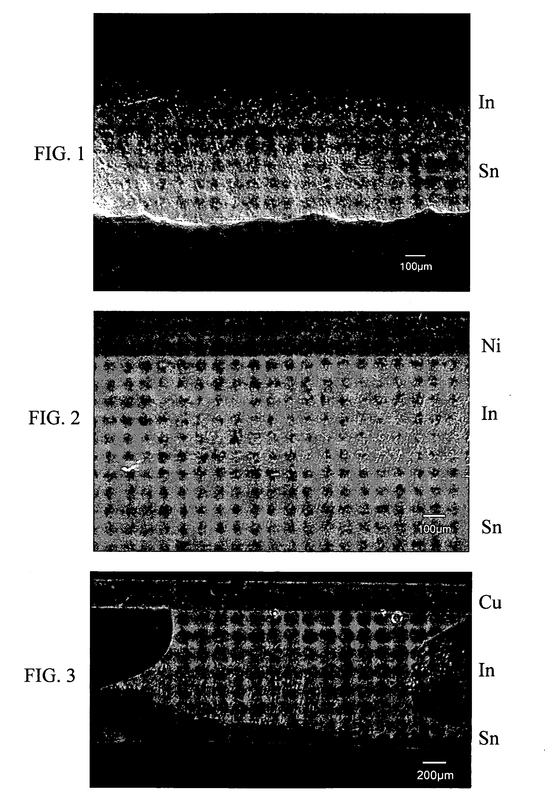
[0011]FIG. 1 is an optical microscopic metallic phase photo showing the cross-section of an In-plated tin substrate formed in

Problems solved by technology

The introduction of a solder with such a high melting point will undoubtly cause changes in the manufacturing processes and energy cost increases in the electronic industry.
However, indium is an expensive material.
Thus, the cost of the Sn—In solder becomes too high, which contributes to the major disadvantage of its use.
It is apparent that a ternary alloy is not easy to be electroplated, and thus will hinder the development of the flip chip technique.
The ternary alloy per se is difficult to be formed by electroplating, and to achieve an accurate control of its composition will be more difficult.
(2003) contains lead and does not comply with the current trend of developing a lead-free solder.
Furthermore, since Bi is very similar to Pb, the toxicity of a Bi-containing solder to human is still under investigation.

Method used


Image

  • Soldering method and solder joints formed therein
  • Soldering method and solder joints formed therein

Examples


example 1

[0046] An acidic electroplating solution of indium sulfate (0.1M) was used to perform plating of indium on the surface of a tin substrate by using Pt as anode, a current density of 3.3 A / dM2, and an operation temperature of 40° C. After one hour, a uniform indium layer with a thickness of about 100 μm was obtained, as shown in FIG. 1.

example 2

[0047] An In-plated tin substrate similar to Example 1 was used to perform a reflow soldering with a nickel substrate at 170° C. The thickness of the indium layer was 500 μm, and the reflow time was 2 minutes. A sound solder joint was formed. A liquid phase reaction portion was seen at the interface between indium and tin. During the soldering process, a liquid phase of indium was formed, and a portion of the tin was also dissolved. A multi-phase region was observed after solidification. Said multi-phase region was a region including said liquid phases of indium and tin, and an interface-reaction region prior to solidification by cooling. As shown in the metallic phase photo of FIG. 2, the multi-phase region is about 80 μm in thickness.

example 3

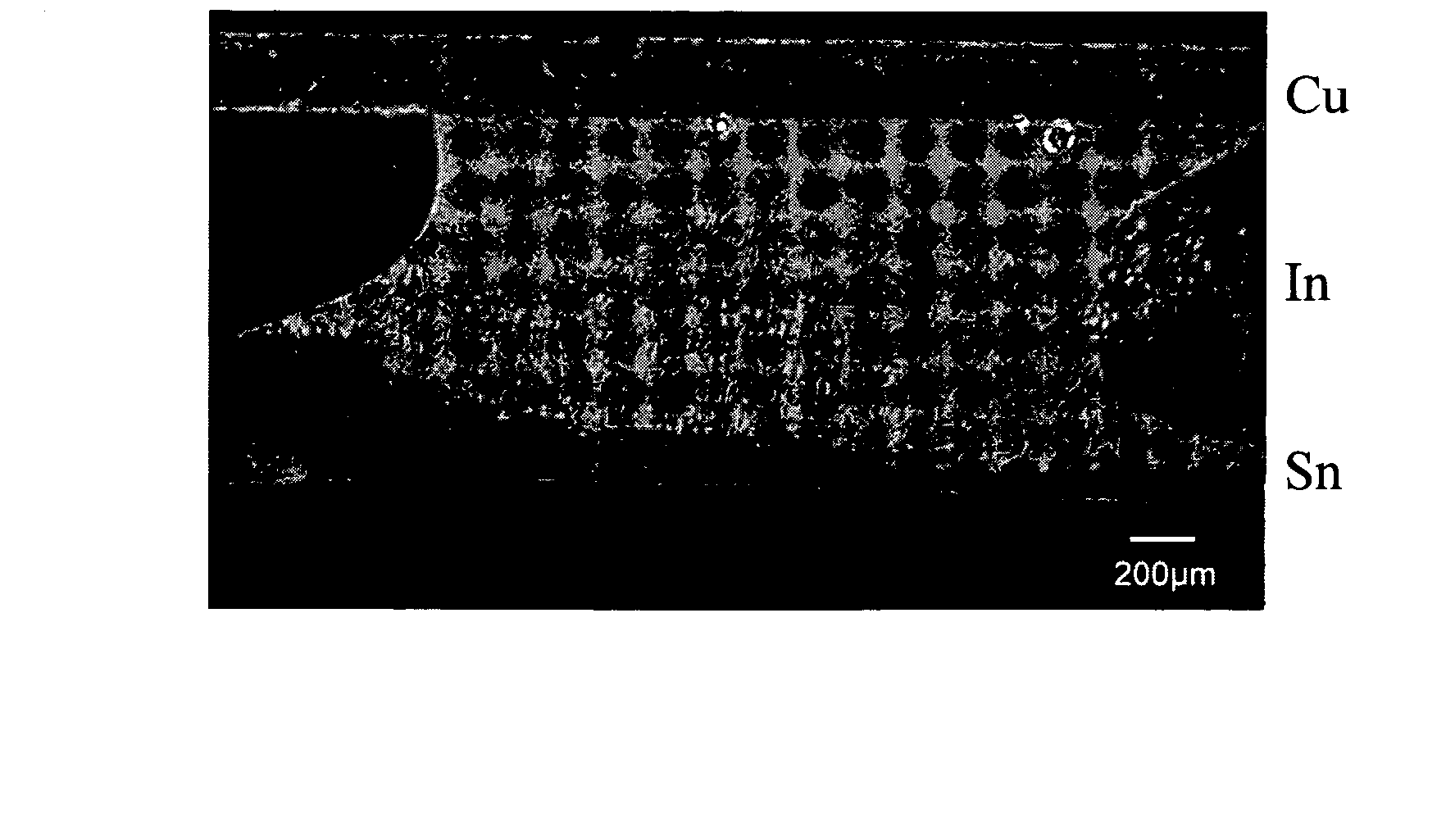
[0048] An In-plated tin substrate similar to Example 1 was used to perform a reflow soldering with a copper substrate at 170° C. The thickness of the indium layer was 500 pin, and the reflow time was 5 minutes. A sound solder joint was formed. A liquid phase reaction portion was seen at the interface between indium and tin. During the soldering process, a liquid phase of indium was formed, and a portion of the tin was also dissolved. A multi-phase region was observed after solidification. Said multi-phase region was a region including said liquid phases of indium and tin, and an interface-reaction region prior to solidification by cooling. As shown in the metallic phase photo of FIG. 3, the multi-phase region is about 80 μm in thickness.


PUM

PropertyMeasurementUnit
melting pointaaaaaaaaaa

Abstract

This invention forms an indium or indium alloy layer on top of a Sn based lead-free solder. The indium or indium alloy layer can be formed by various methods, such as plating, deposition, printing, dipping, etc. The indium-containing layer melts during the soldering process, wets the substrate, and forms a sound solder joint. Since the melting point of indium is 156.6° C., even lower than that of the eutectic Sn—Pb which is at 183° C., so the soldering process can be carried out at a temperature lower than the conventional soldering process. During the soldering process, the indium reacts with the Sn based Pb-free solder alloy. Since the eutectic temperature of Sn—In is at 120° C., during the short time of the soldering process, the surface of the In deposited Pb-free solder remains as the liquid phase and have a good wetting with the substrate, while a In gradient is formed in the In deposited Pb-free solder.

Description

FIELD OF THE INVENTION [0001] The present invention relates to a lead-free solder, and particularly to a lead-free solder formed with an indium or indium alloy layer on the surface thereof. BACKGROUND OF THE INVENTION [0002] Soldering is the most common joining technology used in the electronic industry. The reliability of electronic products is also directly related to the quality of the solder joints. However, due to the concerns of environmental protection and industrial safety, recently there are a lot of efforts in the electronic industry to look for proper lead-free solders to replace the conventional Sn—Pb alloys. At present, the eutectic or near-eutectic Sn—Ag—Cu alloys are the most promising candidates for the lead-free solders. Even though the Sn—Ag—Cu alloy has good properties, its melting point is about 30° C. higher than that of the conventional eutectic Sn—Pb alloy. The introduction of a solder with such a high melting point will undoubtly cause changes in the manufact...

Claims


Application Information

Patent Timeline
Patent Type & Authority Applications(United States)
IPC IPC(8): B23K31/02B23K35/02B23K35/26C22C13/02H01L21/60H05K3/34
CPCB23K35/0238Y10T428/12493B23K35/262C22C13/00H01L24/81H01L2224/13609H01L2224/16H01L2224/8121H01L2224/81815H01L2924/01013H01L2924/01029H01L2924/01049H01L2924/01078H01L2924/01079H01L2924/01082H01L2924/01322H05K3/3463H01L2924/01005H01L2924/01006H01L2924/01033H01L2924/01047H01L2924/0105H01L2924/014H01L2924/01327B23K35/26H01L2924/15747H01L2924/00
Inventor CHEN, SINN-WENLIN, SHIH-KANGYANG, CHING-FENGHUANG, YU-CHIHCHUNG, TING-YINGTSAI, YING-MEIZI, AN-REN
Owner NATIONAL TSING HUA UNIVERSITY
Learn More