
Plasma processing unit

a processing unit and plasma technology, applied in the direction of metal material coating process, electric discharge tube, coating, etc., can solve the problems of inability to install the detector itself in the process vessel, the plasma density is affected, and the plasma processing itself is inappropriate, so as to improve the sensitivity of the pickup antenna, improve the propagation rate, and enhance the sensitivity

Inactive Publication Date: 2005-09-01
TOKYO ELECTRON LTD
View PDF10 Cites 22 Cited by
  • Summary
  • Abstract
  • Description
  • Claims
  • Application Information

AI Technical Summary

Benefits of technology

[0010] The present invention was made in view of the above, and it is an object of the present invention to improve a propagation rate to a pickup antenna of a detector in detecting abnormality in plasma such as abnormal discharge in a process vessel via a through hole, without reducing the thickness of a wall of the process vessel.
[0013] A hole in a prior art is left hollow, and its inner part has an atmosphere whose pressure reduction degree is the same as that in the process vessel, namely, a substantially vacuum atmosphere. Therefore, receiving the electromagnetic wave via the dielectric or filling the hole with the dielectric can improve a propagation rate of an electromagnetic wave, which is generated due to abnormality in plasma such as abnormal discharge, to a pickup antenna. A cutoff frequency in this case becomes lower in inverse proportion to a square root of a dielectric constant. Therefore, a relative dielectric constant of the filled dielectric (dielectric constant of the dielectric / dielectric constant of a vacuum) is preferably as high as possible, and a dielectric such as, for example, a quartz material with a relative dielectric constant of about 3.7 or higher is highly practical.
[0015] In such a structure that the pickup antenna covered with the covering member made of the dielectric is disposed inside the hole, the hole need not be completely filled with the dielectric and thus a gap may exist between the covering member and the inner face of the hole. Such arrangement that the pickup antenna covered with the covering member is inserted in the hole allows the pickup antenna to receive the electromagnetic wave at a position closer to the location of the occurrence of abnormality in plasma such as abnormal discharge than in the prior art. This improves a propagation rate to the pickup antenna, resulting in enhanced sensitivity.
[0016] According to the present invention, it is possible to improve sensitivity of a pickup antenna and to make a frequency band of a cutoff frequency lower than that in a prior art, without any reduction in thickness of a wall of a process vessel or without any increase in size of a hole itself. Consequently, abnormal discharge and an abnormal plasma condition in the process vessel can be detected with higher accuracy than in the prior art.

Problems solved by technology

In the plasma processing, abnormal discharge, if occurring in the plasma generated in the process vessel, may possibly impair uniformity of plasma density and result in inappropriate plasma processing itself.
Such a detector includes an antenna or the like for picking up an electromagnetic wave generated due to the abnormal discharge, but the detector itself cannot be installed in the process vessel.
However, such a through hole functions as a kind of a waveguide for a high-frequency wave, and there may be a case where a signal with a frequency lower than a cutoff frequency (a lower limit frequency at which an electric field propagation rate becomes 1) does not sufficiently reach the pickup antenna.
This limits a signal detector to be used and necessitates an expensive measurement instrument.
Reduction in length of the through hole, in other words, reduction in thickness of the wall of the process vessel would result in an improved propagation rate, but pose a problem in terms of strength of the process vessel itself.

Method used


Image

  • Plasma processing unit
  • Plasma processing unit
  • Plasma processing unit

Examples


Embodiment Construction

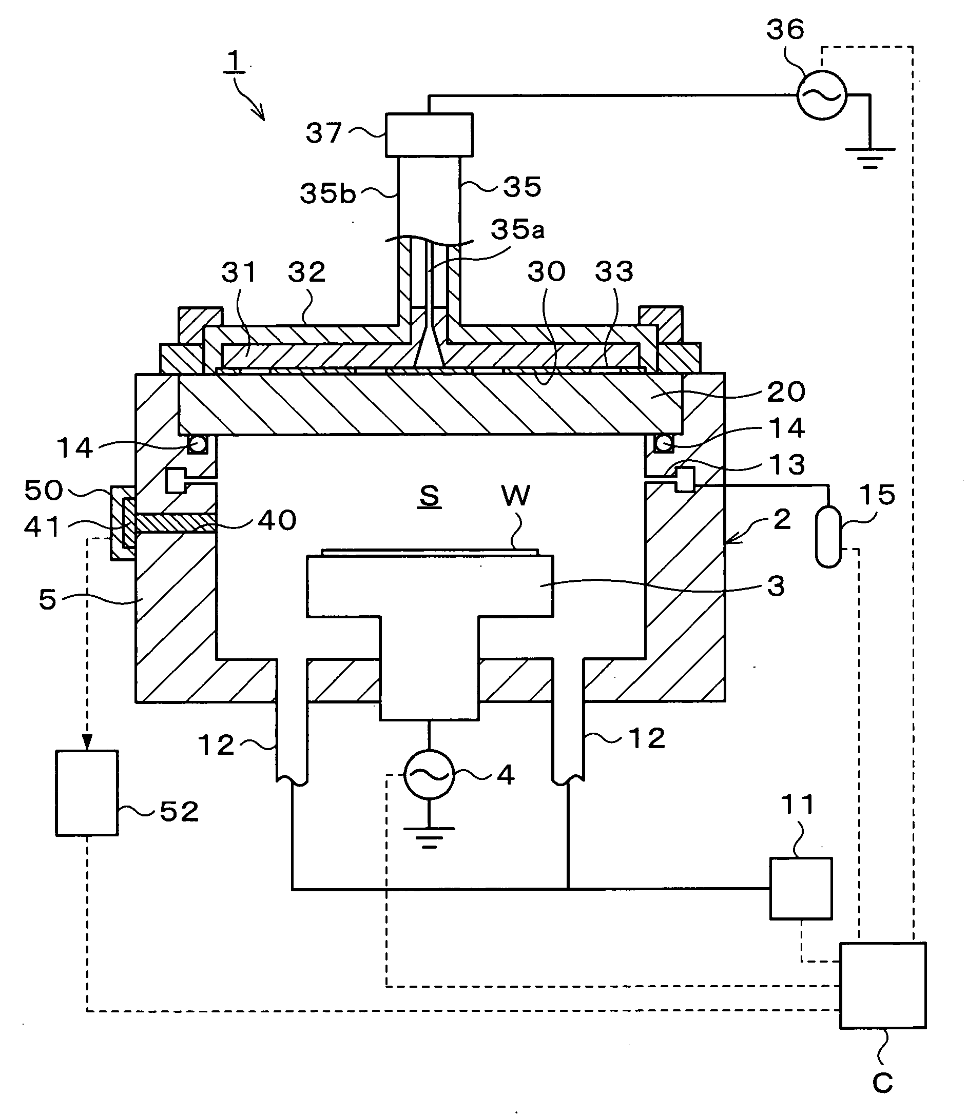
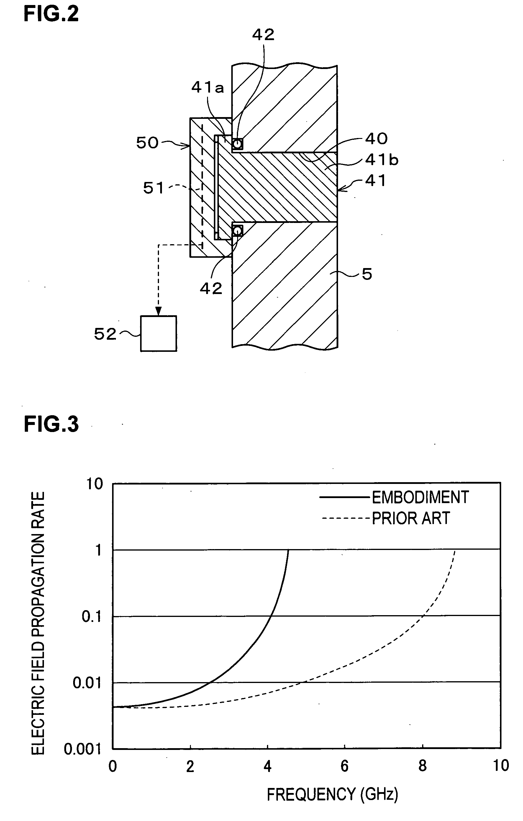
[0024] Hereinafter, an embodiment of the present invention will be described. FIG. 1 shows a vertical cross section of a plasma processing unit 1 according to this embodiment, and this plasma processing unit 1 includes a process vessel 2 made of, for example, aluminum, and formed in a bottomed cylindrical shape with an upper opening. The process vessel 2 is grounded. This process vessel 2 has in a bottom portion thereof a susceptor 3 for placing a substrate, for example, a semiconductor wafer (hereinafter, referred to as a wafer) W. The susceptor 3 is made of, for example, metal such as aluminum and is supplied with a bias high-frequency power from an AC power source 4 provided outside the process vessel 2. The susceptor 3 may be made of ceramics such as AlN, SiC, or the like. Further, the susceptor 3 may have a built-in heater capable of heating the substrate on the susceptor 3.

[0025] The process vessel 2 has in its bottom portion an exhaust pipe 12 through which an atmosphere ins...


PUM

PropertyMeasurementUnit
Lengthaaaaaaaaaa
Dielectric polarization enthalpyaaaaaaaaaa
Sizeaaaaaaaaaa

Abstract

According to the present invention, since the inside of a hole formed in a sidewall of a process vessel of a plasma processing unit is filled with a dielectric, a propagation rate of the electromagnetic wave to a pickup antenna is improved when an electromagnetic wave generated due to abnormality in plasma such as abnormal discharge is to be detected via the hole. Accordingly, it is possible to improve detection sensitivity without any change in size or length of the hole. Consequently, abnormal discharge in plasma processing can be detected with high accuracy.

Description

BACKGROUND OF THE INVENTION [0001] 1. Field of the Invention [0002] The present invention relates to a plasma processing unit. [0003] 2. Description of the Related Art [0004] Conventionally, a plasma processing unit has been proposed that generates plasma in a process vessel through the use of a microwave or other high-frequency wave to apply various kinds of plasma processing such as, for example, CVD processing or etching processing to a substrate placed in the process vessel. [0005] In the plasma processing, abnormal discharge, if occurring in the plasma generated in the process vessel, may possibly impair uniformity of plasma density and result in inappropriate plasma processing itself. Therefore, a system including a detector, which is provided outside a process vessel, for monitoring the condition of plasma has been conventionally been proposed (Japanese Patent Application Laid-open No. Hei 9-266098). When abnormal discharge occurs in the process vessel, this detector detects ...

Claims


Application Information

Patent Timeline
IPC IPC(8): C23C16/00H01J37/32
CPCH01J2237/0206H01J37/32935
Inventor ISHIBASHI, KIYOTAKATIAN, CAI ZHONG
Owner TOKYO ELECTRON LTD
Learn More