
Printed wiring board and semiconductor device

a technology of printed wiring board and semiconductor device, which is applied in the direction of printed circuit stress/warp reduction, circuit inspection/indentification, non-metallic protective coating application, etc., can solve the problem that the mounting of the semiconductor device on the substrate cannot be sure in some cases, and achieve the effect of preventing deformation of the printed wiring board

Inactive Publication Date: 2005-06-23
MITSUI MINING & SMELTING CO LTD
View PDF2 Cites 43 Cited by
  • Summary
  • Abstract
  • Description
  • Claims
  • Application Information

AI Technical Summary

Benefits of technology

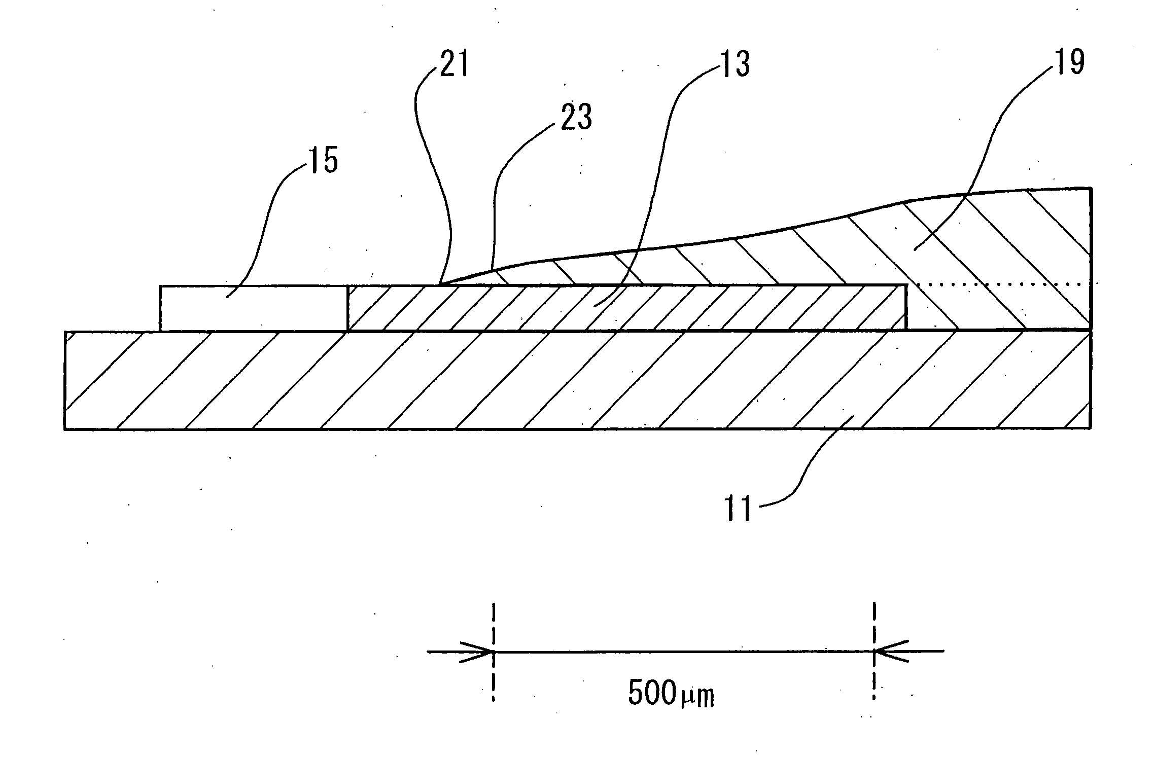
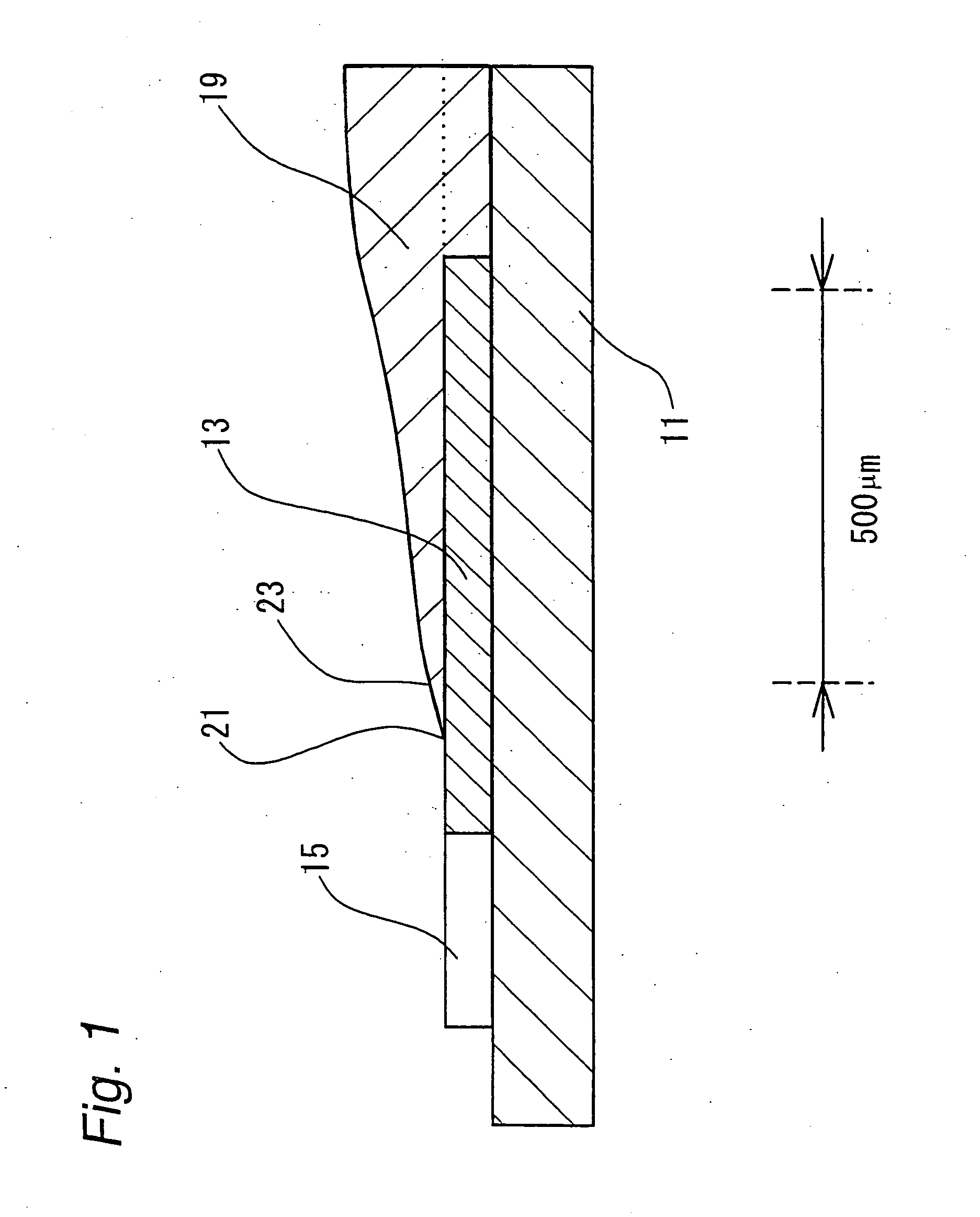
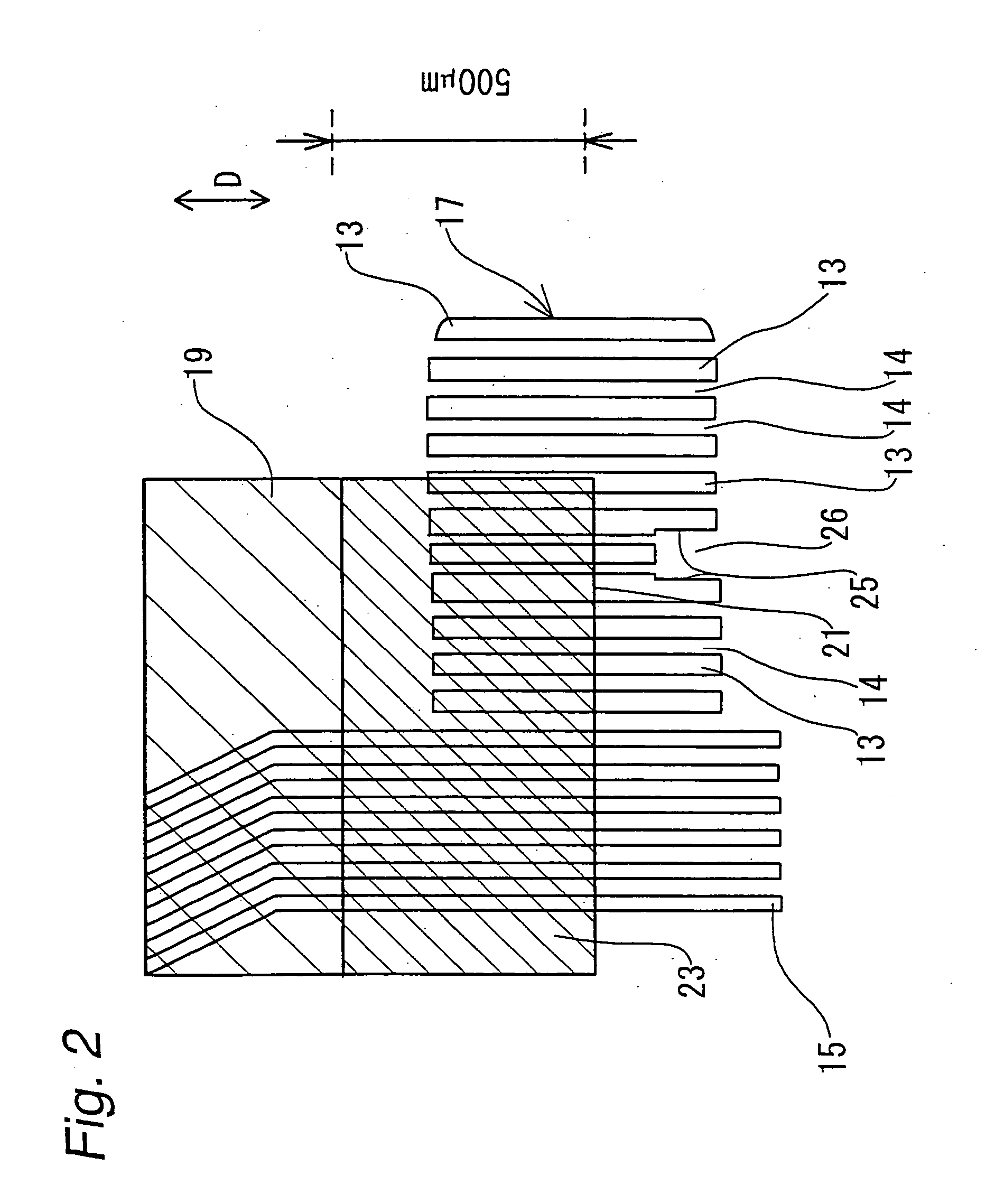
[0064] In the printed wiring board of the invention, a coating thickness control area to control the coating thickness of the solder resist is formed in the dummy pattern, and therefore, a solder resist layer in which the coating thickness is gradually decreased toward the edge of the layer to form a slope can be formed uniformly even on the dummy pattern similarly to that on the wiring pattern.
[0065] Further, even when a solder resist coating thickness control area is formed in the dummy pattern as described above, various functions inherent in the dummy pattern, such as an alignment function and a function of preventing deformation of the printed wiring board due to etching, are not impaired. EXAMPLES
[0066] The printed wiring board and the semiconductor device of the present invention are further described with reference to the following examples, but it should be construed that the invention is in no way limited to those examples.

Problems solved by technology

In the mounting of the semiconductor device on such a substrate, if the thickness of the solder resist layer of the carrier is too large, the edge of the substrate and the solder resist layer come into contact with each other, so that mounting of the semiconductor device on the substrate cannot be surely effected in some cases.

Method used


Image

  • Printed wiring board and semiconductor device
  • Printed wiring board and semiconductor device
  • Printed wiring board and semiconductor device

Examples


example 1

[0067] A laminate consisting of a polyimide film (available from Ube industries, Ltd., Upilex S) having a thickness of 75 μm and an electrodeposited copper foil having a thickness of 18 μm was prepared.

[0068] The surface of the electrodeposited copper foil of the laminate was coated with a photoresist, and the photoresist was exposed and developed to form a lead pattern and a fine wire pattern that was almost parallel to the lead pattern, as shown in FIG. 2. Then, using the thus formed patterns as masking materials, the copper foil was selectively etched with an etching solution to form a prescribed wiring pattern. In the wiring pattern thus formed, such a dummy pattern constituted of a large number of fine wires almost parallel to the outer leads as shown in FIG. 2 was formed by the side of the outer leads. The pitch of the outer leads was 80 μm (lead width: 40 μm, space: 40 μm), and the space between the outermost lead of the outer leads and the dummy pattern was 40 μm. The width...

example 2

[0084] A film carrier was prepared in the same manner as in Example 1, except that the shape of the dummy pattern was changed as shown in FIG. 3. That is to say, at the position 40 μm apart from the edge of the wiring pattern 15 constituted of plural wirings formed in almost parallel to one another, a dummy pattern was formed so that an outer peripheral metal edge 27 became parallel to the plural wirings of the wiring pattern 15. This dummy pattern had a cutout 22 formed in such a manner that a center portion of a solid dummy pattern was removed from the side which did not face the wiring pattern 15. In the dummy pattern, a depression 26 for alignment was formed. The bottom of the depression 26 was connected with the cutout 22, and the outer peripheral metal edge 27 was discontinuous at the position of the depression 26.

[0085] When the edge portion of the above-prepared solder resist layer having a slope length of 500 μm was observed, the solder resist layer had a slope uniformly e...


PUM


Abstract

A printed wiring board has a large number of wirings formed substantially parallel to one another, a dummy pattern is formed along the wirings and a solder resist layer is formed by coating the wirings and the dummy pattern with a solder resist. The coating thickness of said solder resist gradually decreases toward the edge, wherein the dummy pattern has a solder resist coating thickness control area. A semiconductor device includes the above-mentioned printed wiring board with an electronic part mounted thereon. Accordingly, a slope uniformly extending over the whole width of the solder resist layer is formed at the edge portion of the solder resist layer to improve electrical connectivity.

Description

FIELD OF THE INVENTION [0001] The present invention relates to a printed wiring board having a solder resist layer in which the coating thickness of a solder resist is gradually decreased toward the edge to form a slope, and a semiconductor device. More particularly, the invention relates to a printed wiring board having a solder resist layer whose edge portion is in a shape of a slope and having a dummy pattern in a specific shape. BACKGROUND OF THE INVENTION [0002] In order to mount electronic parts, a carrier having a wiring pattern on a surface of an insulating substrate is employed. Such a carrier is formed by a process comprising forming a photosensitive resin layer on a surface of a laminate consisting of an insulating substrate and a conductive metal, exposing and developing the photosensitive resin layer to form a desired pattern, selectively etching the conductive metal using the thus formed pattern as a masking material to form a wiring pattern made of the conductive meta...

Claims


Application Information

Patent Timeline
IPC IPC(8): H05K3/28H05K1/02H05K3/34
CPCH05K1/0266H05K1/0271H05K2203/0594H05K2201/09781H05K3/3452H05K1/02H05K3/28
Inventor FUJII, NOBUAKI
Owner MITSUI MINING & SMELTING CO LTD
Learn More