
Semiconductor device and method of manufacturing the same

a semiconductor and device technology, applied in semiconductor devices, semiconductor/solid-state device details, electrical devices, etc., can solve the problems of affecting the performance of the element, the short channel effect, and the inability to improve the element performance as expected, so as to reduce the area of the source part, reduce parasitic capacitance, and widen the layout design freedom

Inactive Publication Date: 2005-06-09
SEIKO EPSON CORP
View PDF0 Cites 10 Cited by
  • Summary
  • Abstract
  • Description
  • Claims
  • Application Information

AI Technical Summary

Benefits of technology

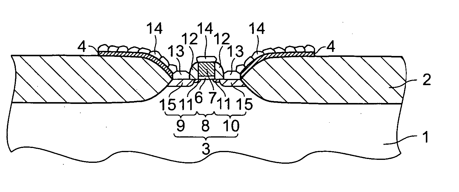
[0016] According to the configuration, by forming the underlayer film including nitrogen on the predetermined region on the element isolation region, the predetermined region extending from the border of the active element forming region to the element isolation region side, a silicon film or a mixed crystal film of silicon and germanium can readily and selectively be formed on the underlayer film. The silicon film or the mixed crystal film of silicon and germanium can readily be turned into a conductive film by ion implantation of a dopant or further making it to be a silicide. Since the conductive film can be electrically connected to the active element, the electrical connection to an electrical wiring can be conducted in the element isolation region, not the active element forming region. This makes it possible to reduce the area of a source part or a drain part, for example, in a MIS field effect transistor. The reduction of the area of the source part and the drain part has an effect of reducing parasitic capacitance. In addition, a raised structure of the source / drain region can suppress a single channel effect and reduce a junction leakage caused by the silicide. Further, since the contact of the source part and the drain part can be located on the LOCOS, there is an effect of widening the layout design freedom.
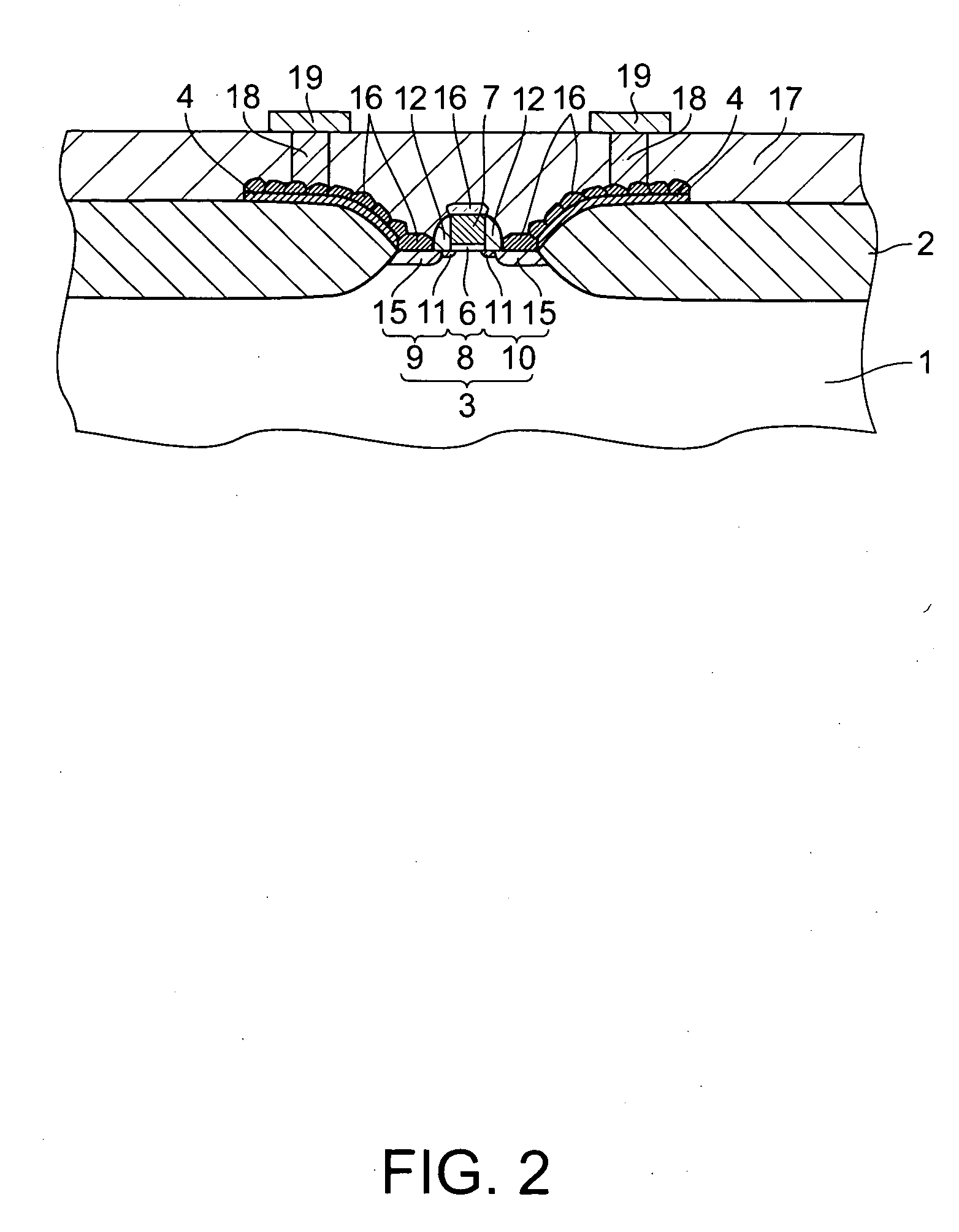
[0040] According to the method, the electrical connection of the active element can be conducted by forming the electrical wiring on the interlayer insulating film and forming the conductive layer so as to be electrically connected to the silicide on the element isolation region. This makes it possible to reduce the area of a source part and a drain part, for example, in the case where the active element is the MISFET. The reduction of the area of the source part and the drain part has an effect of reducing parasitic capacitance. Further, since the contact of the source part and the drain part can be located on the LOCOS, there is an effect of widening the layout design freedom.

Problems solved by technology

However, while an integration degree is increased due to the micro miniaturization, it becomes difficult to improve element performance as expected.
In addition, short channel effect that is an undesirable phenomenon inherent to the miniaturized MISFET becomes predominant.
If nothing is done, understandably, each MISFET is electrically shorted to each other, thereby resulting in malfunction of the circuit.
However, such an element configuration may involve the following problems.
Therefore, in the silicon oxide film 6 formed on the LOCOS 2 as the gate insulating film, leakage currents are large and dielectric breakdowns easily occur.
In addition, since the film thickness of the gate insulating film becomes thinner with miniaturization of the MISFET, deterioration of the film quality of the gate insulating film 6 can adversely affect the characteristics of the MISFET.

Method used


Image

  • Semiconductor device and method of manufacturing the same
  • Semiconductor device and method of manufacturing the same
  • Semiconductor device and method of manufacturing the same

Examples


first embodiment

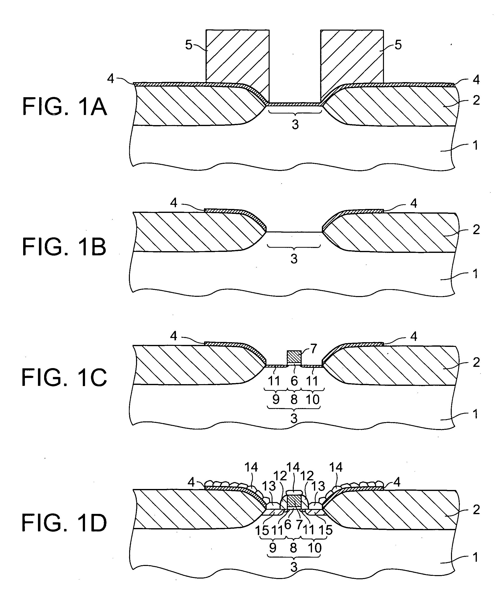
[0051] A first embodiment according to the present invention will now be explained using FIGS. 1 through 4.

[0052]FIGS. 1A through 1D are process sectional views illustrating the manufacturing processes of a MISFET that is the semiconductor device of the first embodiment.

[0053] In FIG. 1A, a forming process of a LOCOS that is an element isolation region, a MISFET forming region that is an active element forming region, and an underlayer film formed by a vapor phase selective epitaxial growth method will be explained. First, the forming process of the LOCOS 2 and the MISFET forming region 3 will be explained. A silicon oxide film (not shown) is formed on the entire surface of a silicon substrate 1. Subsequently, a silicon nitride film (not shown) is formed on the silicon oxide film. The silicon nitride film excluding the part becoming the MISFET forming region 3 is removed so as to expose the silicon oxide film of the part becoming an element isolation region 2. Then, the silicon ox...

second embodiment

[0088] A second embodiment according to the present invention will now be explained using FIGS. 5 and 6.

[0089]FIGS. 5A through 5D are process sectional views illustrating the manufacturing processes of a MISFET that is the semiconductor device of the second embodiment.

[0090] In FIG. 5A, a gate part forming process will now be explained. The method of forming the LOCOS2 and the MISFET forming region 3 is the same as that in FIG. 1A. In the forming process of the gate part 8, the silicon oxide film is formed as the gate insulating film 6 by a thermal oxidation method after forming the LOCOS2 and the MISFET forming region 3. Then, the polysilicon film that is the gate electrode 7 is formed by a CVD method. Next, the gate electrode 7 and the gate insulating film 6 are processed using a photolithography method and a dry etching method so as to form the gate part 8 in the vicinity of the center of the MISFET forming region 3.

[0091] By performing the above-mentioned forming processes of...

third embodiment

[0109] A third embodiment according to the present invention will now be explained using FIGS. 7 and 8.

[0110]FIGS. 7A through 7D are process sectional views illustrating the manufacturing processes of a MISFET that is the semiconductor device of the third embodiment.

[0111] In FIG. 7A, the forming processes of the LOCOS, the MISFET forming region, and protection film for the MISFET forming region will now be explained. A silicon oxide film (not shown) is formed on the entire face of the silicon substrate 1. Subsequently, a silicon nitride film (not shown) is formed on the silicon oxide film. The silicon nitride film excluding the part becoming the MISFET forming region 3 is removed so as to expose the silicon oxide film of the part becoming the element isolation region 2. Then, the silicon oxide is grown to be thicker by performing thermal oxidation in a thermal oxidation furnace. The silicon oxide film grown thicker becomes the LOCOS 2. The above-mentioned processes are the same a...


PUM

PropertyMeasurementUnit
temperatureaaaaaaaaaa

Abstract

A semiconductor device and a method of manufacturing the same are provided. An underlayer film including nitrogen is formed on a predetermined region on an element isolation region, the predetermined region extending from a border of an active element forming region to the element isolation region side. Silicon or a mixed crystal of silicon or germanium is selectively formed on the underlayer film. Then the silicon or the mixed crystal of silicon and germanium is turned into a conductive film by ion implantation of a dopant or further making it to be a silicide. Subsequently, the conductive film formed on the element isolation region is electrically connected to an electrical wiring.

Description

RELATED APPLICATIONS [0001] This application claims priority to Japanese Patent Application No. 2003-410311 filed Dec. 9, 2003 which is hereby expressly incorporated by reference herein in its entirety. BACKGROUND [0002] 1. Technical Field [0003] The present invention relates to a structure of a transistor formed on a semiconductor substrate and a method of manufacturing the same and, more specifically, to an optimum configuration among an electrical wiring and a source part and a drain part of the transistor, and a method of manufacturing the configuration. [0004] 2. Related Art [0005] Due to the demands for highly integrated semiconductor elements, it is desirable to downsize a metal insulator semiconductor field effect transistor (MISFET). In addition, low power consumption and high-speed operation are requested as characteristics of the MISFET. [0006] Because of such demands, elements such as the MISFET are being miniaturized. However, while an integration degree is increased du...

Claims


Application Information

Patent Timeline
Patent Type & Authority Applications(United States)
IPC IPC(8): H01L21/20H01L21/28H01L21/265H01L21/285H01L21/3205H01L21/336H01L21/768H01L23/52H01L29/78
CPCH01L21/28518H01L21/28562H01L29/41783H01L29/665H01L21/0262H01L2924/0002H01L21/02381H01L21/02387H01L21/02532H01L21/02639H01L2924/00
Inventor KANEMOTO, KEI
Owner SEIKO EPSON CORP
Learn More