
Method for forming a thin film and method for fabricating a semiconductor device

a semiconductor and thin film technology, applied in semiconductor devices, chemical vapor deposition coatings, coatings, etc., can solve the problems of degrading mobility, affecting the mobility of semiconductor devices, so as to improve the mobility and reliability of semiconductor devices

Inactive Publication Date: 2005-03-31
SONY CORP
View PDF6 Cites 411 Cited by
  • Summary
  • Abstract
  • Description
  • Claims
  • Application Information

AI Technical Summary

Benefits of technology

The present invention provides a method for forming a thin film and a method for fabricating a semiconductor device that can improve mobility and reliability. The method involves forming a hafnium silicate film on a substrate and carrying out thermal treatment on the hafnium silicate film at a specific temperature to remove hydrogen from the hafnium silicate film without causing a phase separation. This thermal treatment prevents boron penetration and improves the performance of the semiconductor device.

Problems solved by technology

In a case where a high dielectric-constant film (referred to as “High-k film”) is formed by a conventional technique, a fixed charge is generated at an interface between the High-k film and the Si substrate or polycrystalline silicon (Poly-Si) electrode, causing a problem in that shifting of a threshold voltage (Vth) and degrading of the mobility occur.
Further, in a PMOS transistor, a problem occurs in that boron with which the gate electrode is doped penetrates the high dielectric-constant film and diffuses into the substrate side during the subsequent thermal treatment.
It is known that boron penetration is suppressed by addition of nitrogen; however, in a case where nitrogen is added by the conventional technique, nitrogen enters the substrate, causing a problem in that the interface state is increased.

Method used


Image

  • Method for forming a thin film and method for fabricating a semiconductor device
  • Method for forming a thin film and method for fabricating a semiconductor device
  • Method for forming a thin film and method for fabricating a semiconductor device

Examples


example 1

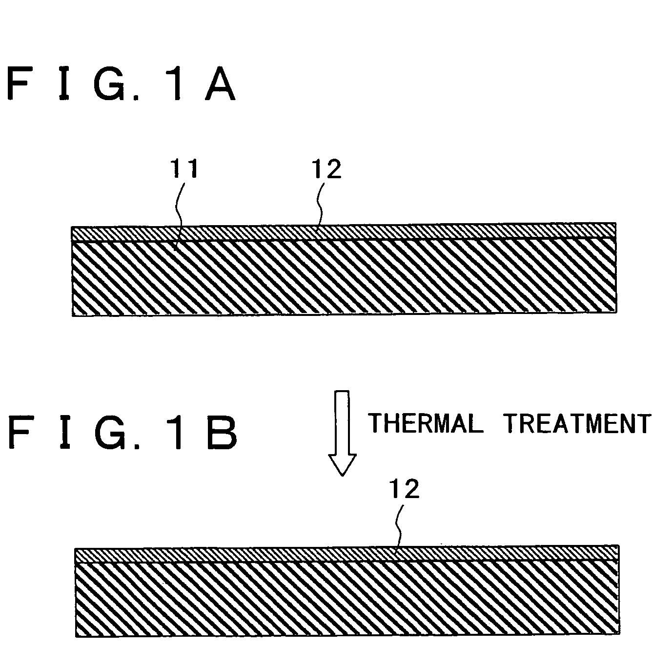
[0023] An embodiment of the method for forming a thin film and the method for fabricating a semiconductor device of the present invention will be described with reference to diagrammatic cross-sectional views of FIG. 1A and FIG. 1B.

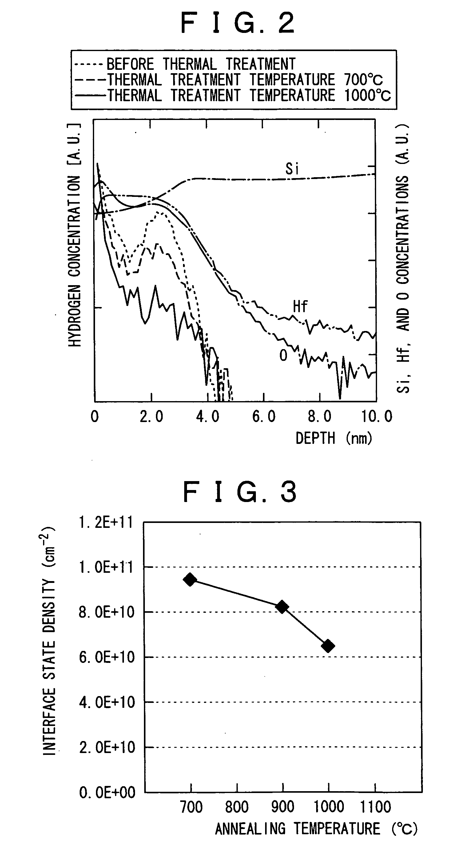
[0024] As shown in FIG. 1A and FIG. 1B, a hafnium silicate (HfSiO) film 12 is formed on a substrate 11 by an atomic layer deposition (ALD) method using an organic raw material. In the substrate 11, a silicon substrate is used as a semiconductor substrate. The hafnium silicate film 12 is formed so that the thickness becomes, for example, 0.5 to 2.0 nm in terms of a silicon oxide film. The hafnium silicate film 12 is formed by an ALD method using an organic raw material, and hence hydrogen remains in the film. Generally, when an insulating film in which hydrogen remains is used in a gate dielectric film, a problem of so-called boron penetration occurs in that boron (B) contained in a polysilicon gate electrode penetrates the gate dielectric film and reache...

example 2

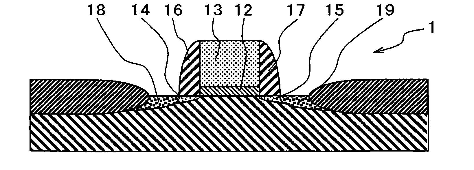
[0031] Next, an embodiment of a method for fabricating a semiconductor device of the present invention will be described with reference to diagrammatic cross-sectional views of FIG. 4A to FIG. 4D.

[0032] As shown in FIG. 4A, a hafnium silicate (HfSiO) film 12 is formed on a substrate 11 by an atomic layer deposition (ALD) method using an organic raw material. In the substrate 11, a silicon substrate is used as a semiconductor substrate. Isolation regions 21 are preliminarily formed in the substrate 11 by a local oxidation method (e.g., a LOCOS method) or an STI (shallow trench isolation) method. The hafnium silicate film 12 is formed so that the thickness becomes, for example, 0.5 to 2.0 nm in terms of a silicon oxide film. The hafnium silicate film 12 is formed by an ALD method using an organic raw material, and hence hydrogen remains in the film. Generally, when an insulating film in which hydrogen remains is used in a gate dielectric film, a problem of so-called boron penetration...


PUM

PropertyMeasurementUnit
gate lengthaaaaaaaaaa
thicknessaaaaaaaaaa
thicknessaaaaaaaaaa

Abstract

By conducting a high temperature annealing in a nitrogen atmosphere at a temperature at which a hafnium silicate film undergoes no phase separation, hydrogen contained in the film is removed and prevention of boron penetration is made possible. The present invention provides a method for forming a thin film including a step of forming a hafnium silicate film on a substrate by an atomic layer deposition method and a step of carrying out thermal treatment on the hafnium silicate film at a thermal treatment temperature equal to or higher than a temperature at which hydrogen contained in the hafnium silicate film is removed and lower than a temperature at which the hafnium silicate film undergoes no phase separation, and a method for fabricating a semiconductor device for forming a gate dielectric film using the method for forming a thin film.

Description

CROSS REFERENCES TO RELATED APPLICATIONS [0001] The present document is based on Japanese Priority Document JP 2003-302291, filed in the Japanese Patent Office on Aug. 27, 2003, the entire contents of which being incorporated herein by reference. BACKGROUND OF THE INVENTION [0002] 1. Field of the Invention [0003] The present invention relates to a method for forming a thin film, which is advantageously used in forming a high-quality hafnium silicate film, and a method for fabricating a semiconductor device using the method for forming a thin film in a process for forming a gate dielectric film. [0004] 2. Description of Related Art [0005] An insulated gate field effect transistor has already been on a stage in which miniaturization thereof is about to achieve a gate length of 0.1 μm. The miniaturization further increases the speed of a device, lowers the power consumption, and reduces the area occupied by a device. In addition, recently, an increased number of devices can be mounted ...

Claims


Application Information

Patent Timeline
Patent Type & Authority Applications(United States)
IPC IPC(8): C23C16/42C23C16/56H01L21/28H01L21/314H01L21/316H01L21/336H01L29/51H01L29/78
CPCH01L21/28185H01L21/28194H01L21/28202H01L29/518H01L21/31645H01L29/517H01L21/3141H01L21/02148H01L21/0228H01L21/02181H01L21/18H01L21/02329H01L21/02337
Inventor HIRANO, TOMOYUKI
Owner SONY CORP
Learn More