Thin germanium oxynitride gate dielectric for germanium-based devices

a technology of germanium-based devices and gate dielectrics, which is applied in the direction of basic electric elements, electrical apparatus, and semiconductor devices, can solve the problems of gate dielectrics, no reliable high-quality gate dielectrics have been found for ge-based materials, and complicated situations

Inactive Publication Date: 2005-03-31
GLOBALFOUNDRIES INC
View PDF17 Cites 11 Cited by
  • Summary
  • Abstract
  • Description
  • Claims
  • Application Information

AI Technical Summary

Benefits of technology

[0006] The present invention offers a solution for the problem of growing a thin germanium oxynitride layer in a controlled manner. The solution involves using a two step process. The first step being incorporating a first concentration of nitrogen into a surface layer underneath a first surface of the Ge-based material. This nitrogen-rich region acts as a diffusion / reaction barrier that controls the germanium oxidation / oxynitridation rate in a second, oxidation step. Such a control allows one to grow ultrathin germanium oxynitrides in a governable, reproducible manner. The thin germanium oxynitride gate dielectric allows for improved properties and higher performance in Ge-based field effect devices.
[0010] It is a further object of the present invention to teach processors which comprise chips containing such a Ge-based field effect device having preferably below 6 nm of EOT, good quality germanium oxynitride gate insulator layers on Ge-based materials.

Problems solved by technology

Gate dielectrics is one of the main problems for MOS field effect device scaling.
In Ge-based devices, the situation is quite complicated.
So far no reliable high-quality gate dielectric has been found for Ge based materials.
Germanium oxide is of poor quality and is soluble in water.
Germanium oxynitride quality and scaling potential up to now was thought to be inferior to the SiO2 / Si system.
This makes it difficult to grow thin germanium oxynitride films with good process control, and / or with an equivalent oxide thickness (EOT) of below about 6 nm.

Method used


Image

  • Thin germanium oxynitride gate dielectric for germanium-based devices
  • Thin germanium oxynitride gate dielectric for germanium-based devices
  • Thin germanium oxynitride gate dielectric for germanium-based devices

Examples


Embodiment Construction

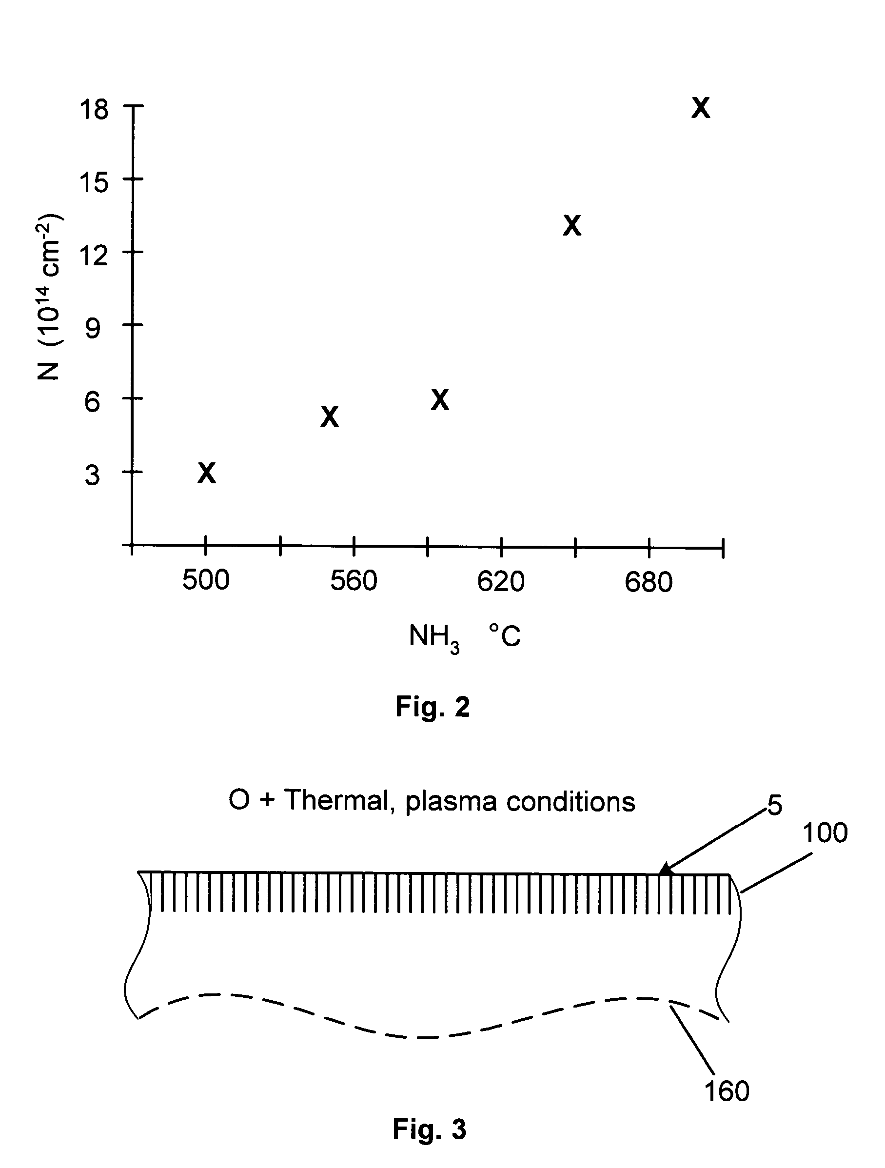
[0018] In the fabrication of high performance Ge-based field effect devices the processing steps that preceded the production of the gate dielectric are known in the art. These steps, such as device isolation, dopant well formation, etc., are assumed to have been completed before commencing the steps of the present invention. However, before the disclosed method steps can take place to produce an the thin germanium oxynitride layer, a surface, referred to as a first surface, of the Ge based material, generally a wafer, the one which will be the recipient of the gate dielectric, has to be properly cleaned. In a representative embodiment such cleaning steps can include, but are not limited to, at least one cycle of oxidation and germanium oxide removal. The oxidation is preferably performed in H2O2 solutions, while oxide removal is accomplished by HF, or HCl, or their mixtures. After the cleaning step the first surface of the Ge based material, which is host to the devices, is ready f...


PUM

PropertyMeasurementUnit
thicknessaaaaaaaaaa
temperatureaaaaaaaaaa

Abstract

A method for producing thin, below 6 nm of equivalent oxide thickness, germanium oxynitride layer on Ge-based materials for use as gate dielectric is disclosed. The method involves a two step process. First, nitrogen is incorporated in a surface layer of the Ge-based material. Second, the nitrogen incorporation is followed by an oxidation step. The method yields excellent thickness control of high quality gate dielectrics for Ge-based field effect devices, such as MOS transistors. Structures of devices having the thin germanium oxynitride gate dielectric and processors made with such devices are disclosed, as well.

Description

FIELD OF THE INVENTION [0001] The present invention relates to electronic devices and systems. In particular it relates to a method of producing a germanium oxynitride layer for use as a thin gate dielectric. BACKGROUND OF THE INVENTION [0002] Today's integrated circuits include a vast number of devices. Smaller devices are key to enhance performance and to improve reliability. As MOS (Metal Oxide Semiconductor Field-Effect-Transistor, a name with historic connotations meaning in general an insulated gate Field-Effect-Transistor) devices are being scaled down, the technology becomes more complex and new methods are needed to maintain the expected performance enhancement from one generation of devices to the next. SUMMARY OF THE INVENTION [0003] Gate dielectrics is one of the main problems for MOS field effect device scaling. This is true for both conventional silicon devices and more advanced (e.g. SiGe, Ge) devices. [0004] In Ge-based devices, the situation is quite complicated. Th...

Claims


Application Information

Patent Timeline
Patent Type & Authority Applications(United States)
IPC IPC(8): H01L21/28H01L21/314H01L21/316H01L21/318H01L29/51
CPCH01L21/02247H01L21/02326H01L21/02337H01L21/0234H01L21/28202Y10S438/933H01L21/3143H01L21/31658H01L21/318H01L29/518Y10S438/906H01L21/28255
Inventor GOUSEV, EVGENISHANG, HUILINGD'EMIC, CHRISTOPHER P.KOZLOWSKI, PAUL M.
Owner GLOBALFOUNDRIES INC
Why Eureka
Try Eureka