Doubled-sided and multi-layered PCD and PCBN abrasive articles
a technology of pcbn and abrasives, applied in the field of abrasive tools, can solve the problems of increasing the thickness of the typical pcd/pcbn layer, so as to improve the cutting and abrasive properties, increase the effective thickness, and tailor the effect of the abrasive properties
- Summary
- Abstract
- Description
- Claims
- Application Information
AI Technical Summary
Benefits of technology
Problems solved by technology
Method used
Image
Examples
example 1
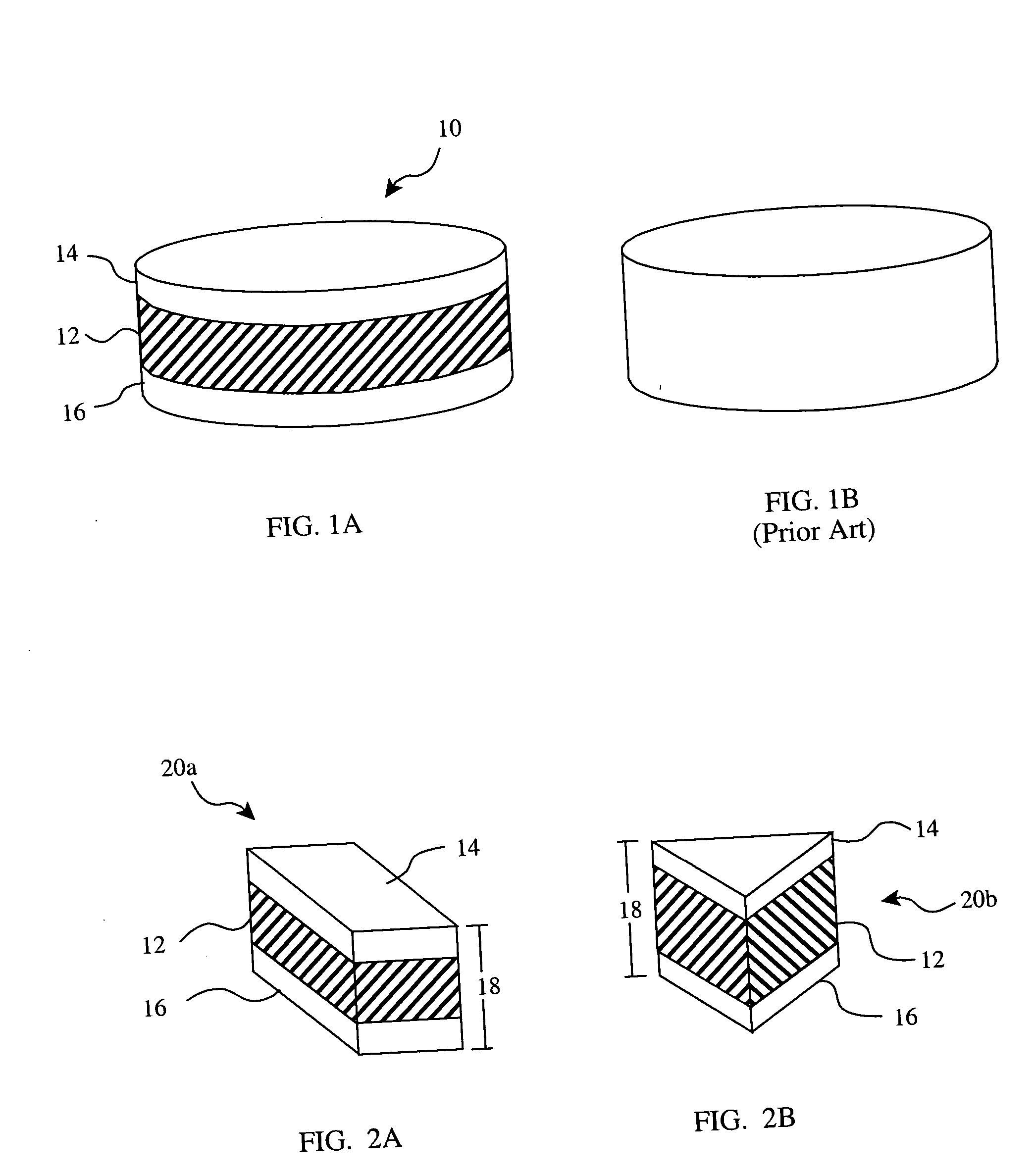
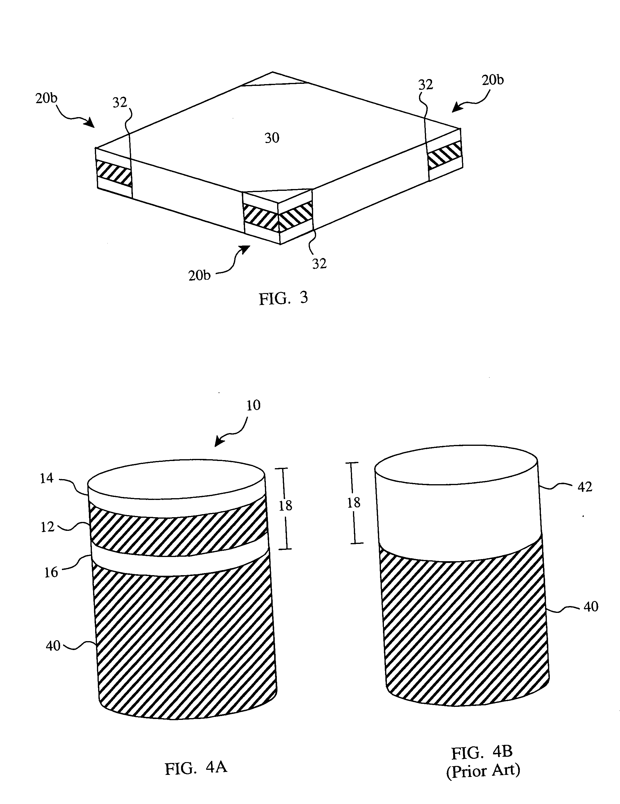
[0067] A layer of CBN particles was mixed with titanium carbide metal and ceramic binder having an average particle size of about 3 μm. The mixture was then placed in a tantalum cup having an inner diameter of 51 mm to a thickness of about 1.5 mm. A cylindrical cobalt cemented tungsten carbide substrate having a thickness of 3 mm was then placed over the layer of CBN. A second layer of CBN having an average particle size of about 3 μm was mixed with TiC and TiN powders was then placed on top of the substrate to a thickness of about 1.5 mm to form a precursor assembly. The precursor assembly was then placed in a HTHP belt apparatus and pressed to about 5 GPa and heated to about 1,400° C. for about 30 minutes. The mixture of CBN and titanium carbide was sintered under HPHT to form chemical bonds between CBN particles and TiC particles. The PCBN sintered mass was then allowed to cool and removed from the apparatus. The sintered PCBN was finished by conventional grinding and lapping pro...
example 2
[0068] A layer of diamond particles having an average particle size of about 30 μm was placed in a tantalum cup having an inner diameter of 35 mm to a thickness of about 1.5 mm. A cylindrical cobalt cemented tungsten carbide substrate having a thickness of 1.0 mm was then placed over the layer of diamond. A second layer of diamond also having an average particle size of about 4 μm was then placed on top of the substrate to a thickness of about 1.5 mm and then another piece of cylindrical cobalt cemented tungsten carbide substrate having a thickness of about 11 mm was placed on the second layer of diamond to form a precursor assembly. The precursor assembly was then placed in a HPHT belt apparatus and pressed to about 5 GPa and heated to about 1,400° C. for about 30 minutes. The cobalt infiltrated from each of the cemented tungsten carbide substrates to sinter each diamond layers together, thus attaching the layers to the adjacent substrates to form a PCD having multiple PCD layers. ...
example 3
[0069] A layer of CBN particles having an average particle size of about 1.0 μm mixed with titanium nitride was placed in a tantalum cup having an inner diameter of 51 mm to a thickness of about 1.5 mm. A cobalt cemented tungsten carbide substrate having a thickness of 1.2 mm was then placed over the layer of CBN particles. A second layer of CBN particles having an average particle size of about 1.0 μm mixed with titanium carbide and titanium nitride sintering aids was then placed on top of the substrate to a thickness of about 1.5 mm to form a precursor assembly. The precursor assembly was then placed in a HPHT belt apparatus and pressed to about 5 GPa and heated to about 1,300° C. for about 20 minutes. The CBN particles sintered together in the presence of the sintering aids to form a double-sided PCBN compact. The sintered mass was then allowed to cool and removed from the apparatus. The PCBN compact was then finished into several 3.2 mm diameter double-sided PCBN blanks having a...
PUM
| Property | Measurement | Unit |
|---|---|---|
| particle size | aaaaa | aaaaa |
| particle size | aaaaa | aaaaa |
| particle size | aaaaa | aaaaa |
Abstract
Description
Claims
Application Information
 - R&D
- Intellectual Property
- Life Sciences
- Materials
- Tech Scout
- Unparalleled Data Quality
- Higher Quality Content
- 60% Fewer Hallucinations
Browse by: Latest US Patents, China's latest patents, Technical Efficacy Thesaurus, Application Domain, Technology Topic, Popular Technical Reports.
© 2025 PatSnap. All rights reserved.Legal|Privacy policy|Modern Slavery Act Transparency Statement|Sitemap|About US| Contact US: help@patsnap.com


