Semiconductor device and method of manufacturing the same
a technology of semiconductor devices and semiconductors, applied in semiconductor devices, semiconductor/solid-state device details, electrical devices, etc., can solve the problems of reducing the thickness of the bit line mask layer, limiting the gap-fill margin, and difficult to form a minute contact hol
- Summary
- Abstract
- Description
- Claims
- Application Information
AI Technical Summary
Problems solved by technology
Method used
Image

Examples
first embodiment
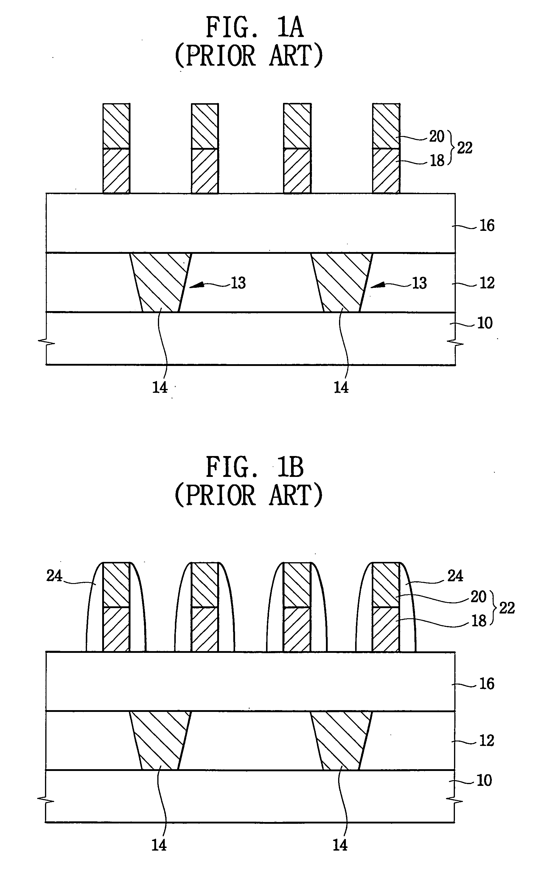
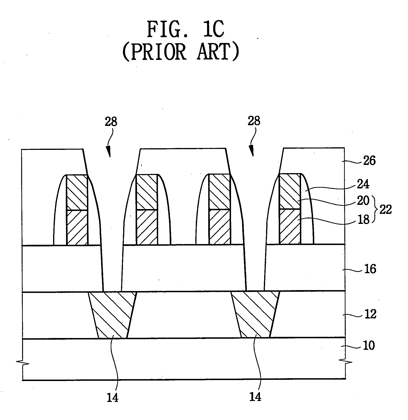
[0043] FIGS. 2A to 2F are cross-sectional views illustrating a method of manufacturing a semiconductor device according to the present invention.
[0044] Referring to FIG. 2A, a first insulating film 52, a conductive film 53, and a second insulating film 55 are successively formed on a semiconductor substrate 50. That is, a silicon oxide based material is deposited on the semiconductor substrate 50 to form the first insulating film 52, and then the conductive film 53 is formed on the first insulating film 52. Preferably, the conductive film 53 includes a composite film that has a first film composed of a first metal and / or a compound of the first metal, e.g., titanium (Ti) / titanium nitride (TiN), and a second film composed of a second metal, e.g., tungsten (W). Next, silicon nitride is deposited on the conductive film 53 to form the second insulating film 55.
[0045] Alternatively, before forming the conductive film 53, the first insulating film 42 can be partially etched by a photolith...
embodiment 2
[0064] FIGS. 3A and 3B are cross-sectional views illustrating a method of manufacturing a semiconductor device according to a second embodiment of the present invention. The method of the present embodiment is substantially similar to embodiment 1 except it specifies planarizing the third insulating film 61 until the surfaces of the wiring 58 is exposed.
[0065] Referring to FIG. 3A, with processes substantially identical to those described in FIGS. 2A and 2B, after a first insulating film 52 is formed on a semiconductor substrate 50, the wiring 58 including conductive film patterns 54 and second insulating film patterns 56 are formed on the first insulating film 52.
[0066] Then, a silicon oxide based material is deposited on a surface of the resultant structure including the wiring 58 to form a third insulating film 61. Using a planarization process, such as a CMP process or an etch-back process, the third insulating film 61 is partially removed until the surfaces of the second insula...
embodiment 3
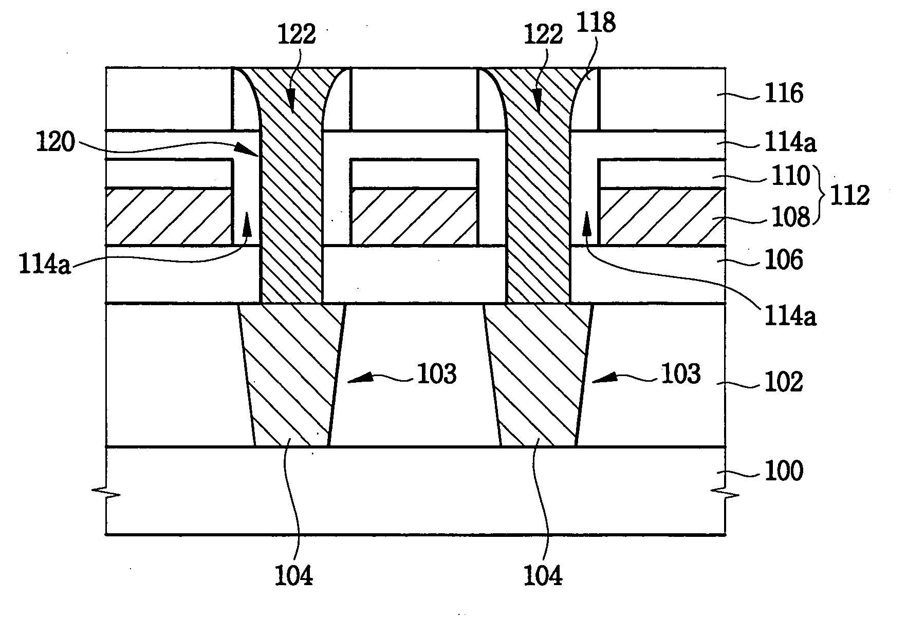
[0073] FIG. 4 is a cross-sectional view of a DRAM device in accordance with a third embodiment of the present invention.
[0074] Referring to FIG. 4, metal oxide semiconductor (MOS) transistors (not shown) having gate electrodes for word lines, capacitor contact regions (source regions), and bit line contact regions (drain regions), are formed on a semiconductor substrate 100. Each gate electrode includes a gate insulating film, a gate capping film composed of silicon nitride and a gate sidewall spacer composed of silicon nitride.
[0075] An interlayer dielectric film 102, composed of silicon oxide, is formed on the substrate 100 to cover the MOS transistors. Contact holes 103 penetrate the interlayer dielectric film 102 to expose the source / drain regions. The contact holes 103 are self-aligned relative to the gate electrodes, respectively. Pad electrodes 104, composed of doped polysilicon, are formed in the self-aligned contact holes 103, respectively. The pad electrodes 104 are node-s...
PUM
 Abstract
Description
Claims
Application Information
 - R&D
- Intellectual Property
- Life Sciences
- Materials
- Tech Scout
- Unparalleled Data Quality
- Higher Quality Content
- 60% Fewer Hallucinations
Browse by: Latest US Patents, China's latest patents, Technical Efficacy Thesaurus, Application Domain, Technology Topic, Popular Technical Reports.
© 2025 PatSnap. All rights reserved.Legal|Privacy policy|Modern Slavery Act Transparency Statement|Sitemap|About US| Contact US: help@patsnap.com