Laser module and production process thereof
a technology of laser module and production process, which is applied in the direction of lasers, semiconductor laser arrangements, semiconductor lasers, etc., can solve the problems of optical loss of optical components included in optical modules, optical loss thought to occur, and optical loss of optical components
- Summary
- Abstract
- Description
- Claims
- Application Information
AI Technical Summary
Problems solved by technology
Method used
Image
Examples
first embodiment
[0099] Herebelow, the present invention will be described in detail with reference to the drawings.
[0100] Module Structure
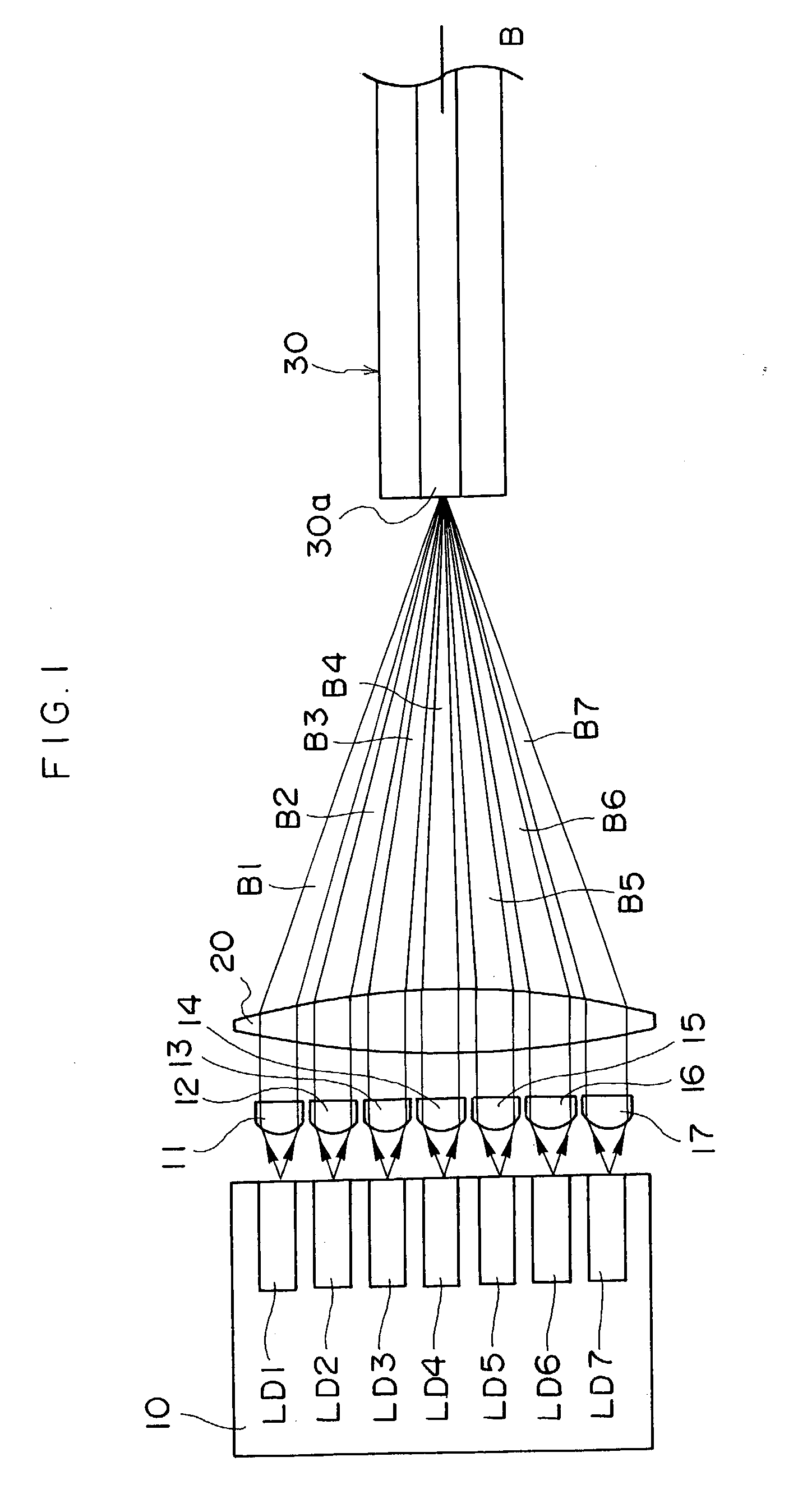
[0101] A laser module relating to the first embodiment is provided with a multiplex laser light source shown in FIG. 1. This multiplex laser light source is structured with a plurality of chip-form lateral multimode gallium-nitride (GaN)-related semiconductor lasers LD1, LD2, LD3, LD4, LD5, LD6 and LD7, collimator lenses 11, 12, 13, 14, 15, 16 and 17, a single condensing lens 20, and a single multimode optical fiber 30. The GaN-related semiconductor lasers LD1 to LD7 are fixedly arranged on a heat block 10. The collimator lenses 11 to 17 are provided in correspondence with the GaN-related semiconductor lasers LD1 to LD7, respectively.
[0102] The GaN-related semiconductor lasers LD1 to LD7 all have a common oscillation wavelength (for example, 405 nm), and a common maximum output (for example, 100 mW). For the GaN-related semiconductor lasers LD1 to LD7, lasers can...
second embodiment
[0126] Now, the present invention will be described in detail using the drawings.
[0127] A can-form sealed laser module according to the second embodiment of the present invention will be described. FIG. 8 shows a schematic structural view of this laser module, FIG. 9A shows a schematic plan view, and FIG. 9B shows a schematic side view.
[0128] As shown in FIG. 8, in the laser module according to the present embodiment, a heat sink 104, an electrode terminal 108 and a monitoring photodiode 110 are fixed on a stem 101. A semiconductor laser element 106 on a submount 105 is adhered to the heat sink 104. The electrode terminal 108 is connected with the semiconductor laser element 106 by a wire 109. The monitoring photodiode 110 is connected to an electrode terminal 112 by a wire 113. Furthermore, a single zeolite adsorbent 111 is fixed on the stem 101 by an inorganic adhesive. These components are covered by a container 102 which is provided with a glass window 103 to which a non-reflect...
third embodiment
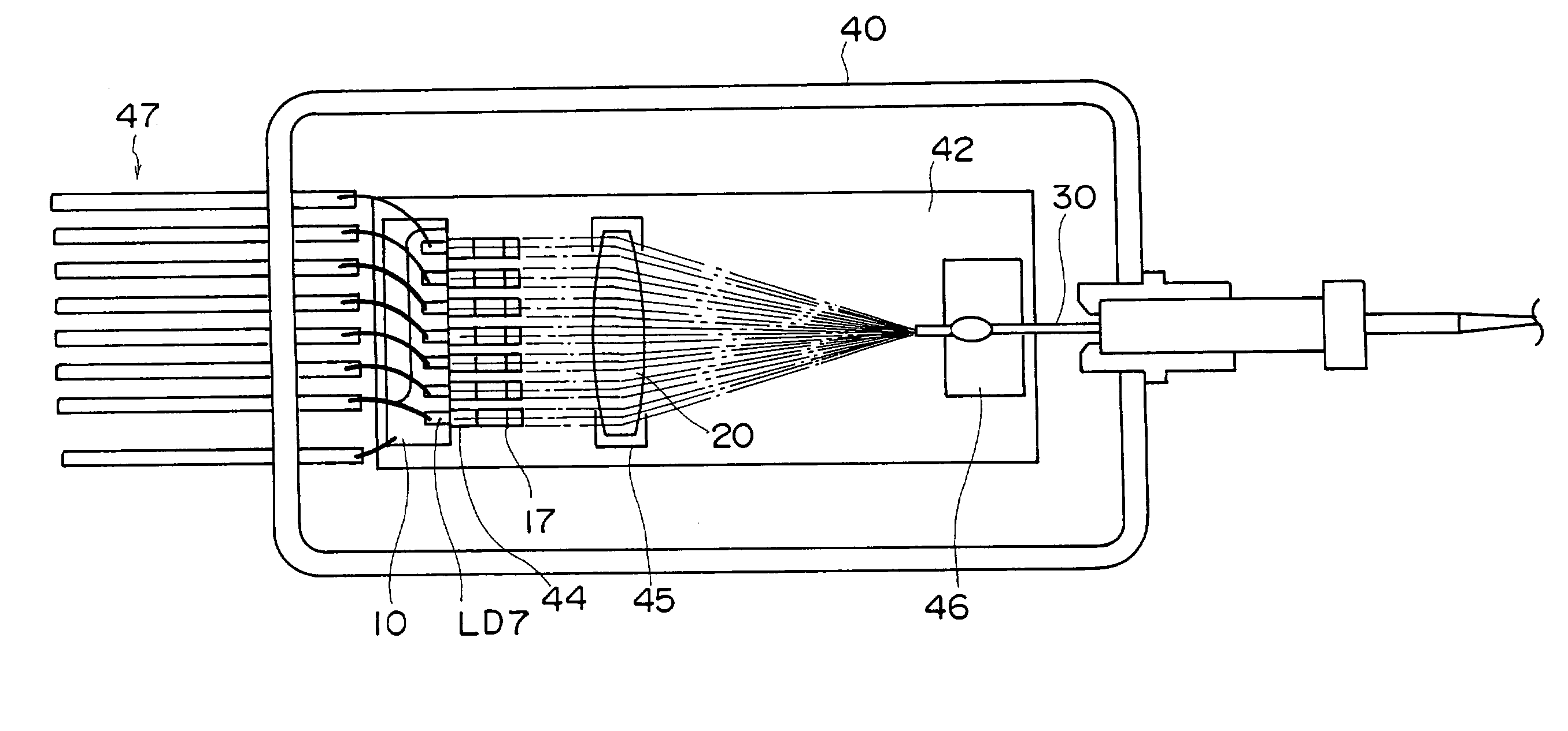
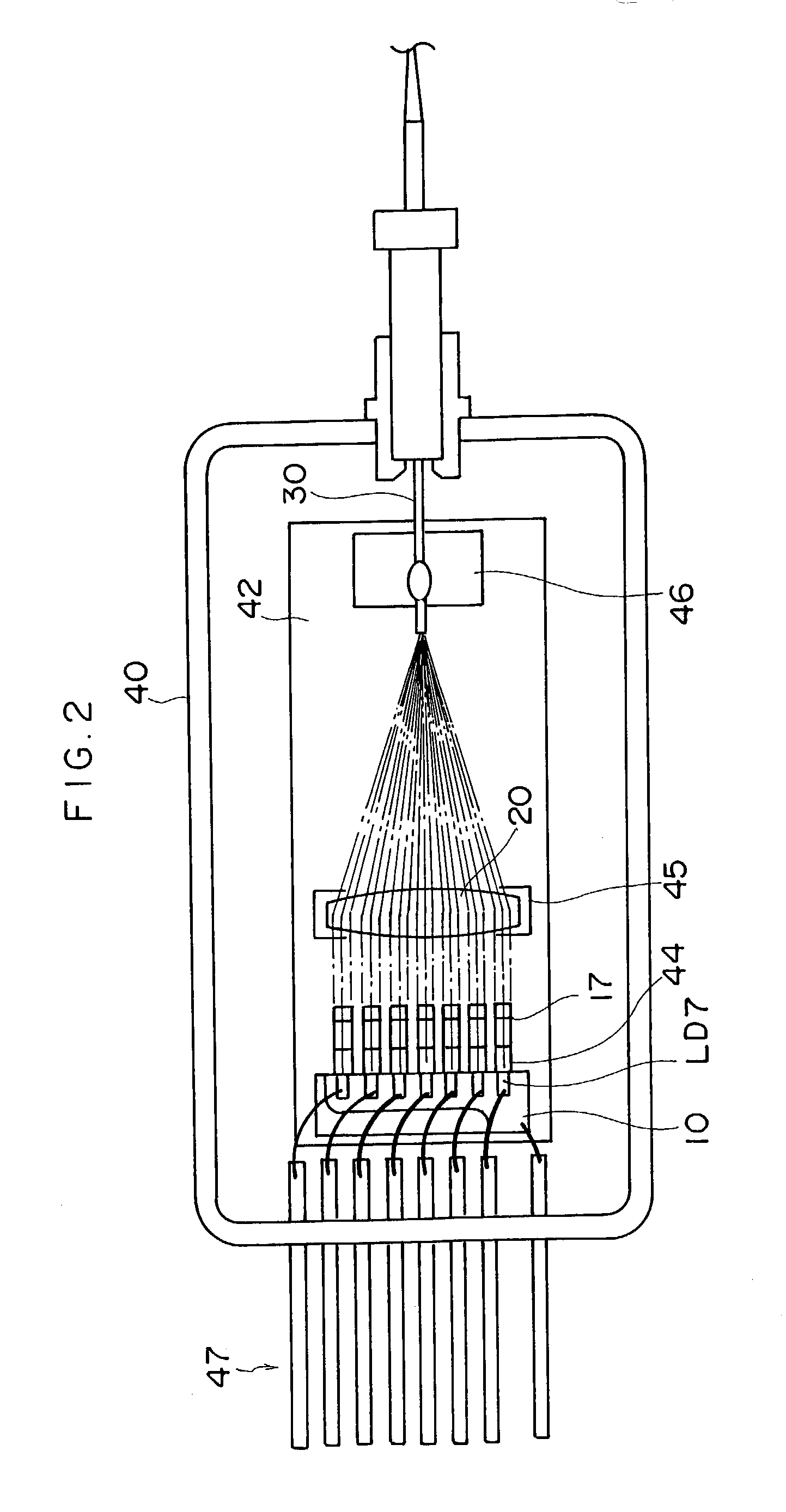
[0137] Next, a laser module according to the present invention will be described. A schematic side view and plan view of this laser module are shown in FIGS. 12A and 12B.
[0138] As shown in FIGS. 12A and 12B, in the laser module according to the present embodiment, a base plate 142 is fixed at a floor face of a container 140. A heat block 120, collimator lenses 131, 132, 133, 134, 135, 136 and 137, a condensing lens 143 and a multimode optical fiber 130 are fixedly disposed on the base plate 142. Seven GaN-related semiconductor laser elements LD121, LD122, LD123, LD124, LD125, LD126 and LD127 are adhered to the heat block 120. The collimator lenses 131 to 137 are held at collimator lens holders 144, which are attached to the heat block 120. The condensing lens 143 is held at a condensing lens holder 145, and the multimode optical fiber 130 is held at a fiber holder 146. Openings are formed in a wall face of the container 140. Wiring 147, which supplies driving current to the GaN-rela...
PUM
 Abstract
Description
Claims
Application Information
 - R&D
- Intellectual Property
- Life Sciences
- Materials
- Tech Scout
- Unparalleled Data Quality
- Higher Quality Content
- 60% Fewer Hallucinations
Browse by: Latest US Patents, China's latest patents, Technical Efficacy Thesaurus, Application Domain, Technology Topic, Popular Technical Reports.
© 2025 PatSnap. All rights reserved.Legal|Privacy policy|Modern Slavery Act Transparency Statement|Sitemap|About US| Contact US: help@patsnap.com


