Chip resistor
a chip resistor and resistor technology, applied in the field of chip resistors, can solve the problems of inability to solve the problem, inability to use ni--cr or ni--ti, and loss of thin films made of ni--cr
- Summary
- Abstract
- Description
- Claims
- Application Information
AI Technical Summary
Problems solved by technology
Method used
Image
Examples
first embodiment
[0023] First Embodiment
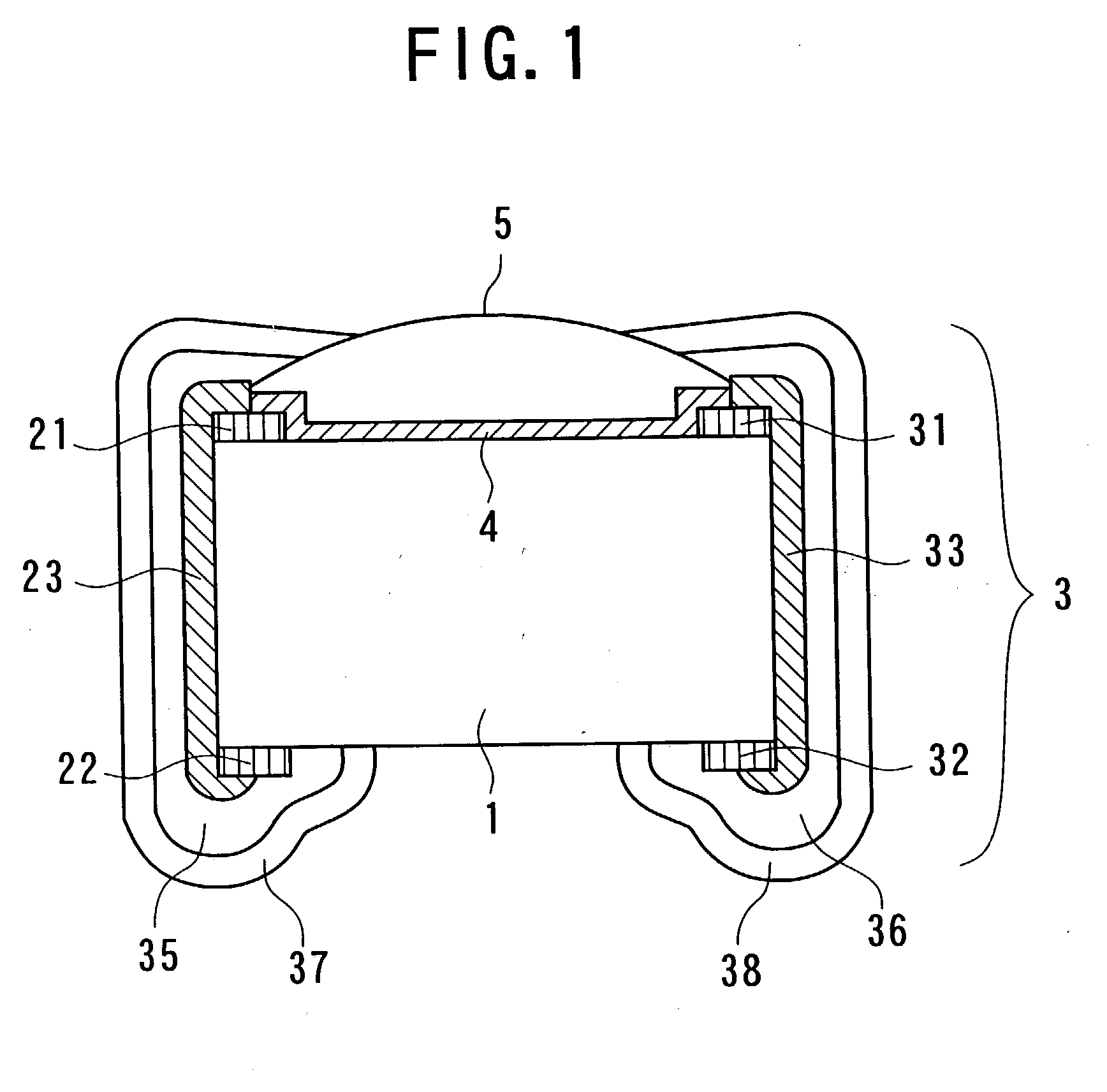
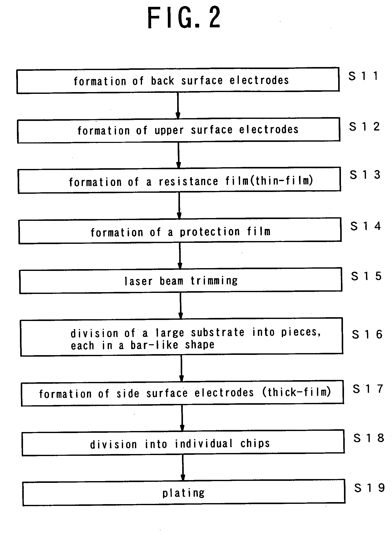
[0024] As schematically shown in FIG. 1, with a chip resistor according to a first embodiment, there are provided upper surface electrodes 21, 31, formed of a thick-film, and back surface electrodes 22, 32, formed of a thick-film, at opposite ends of the top surface and back surface of an insulating substrate 1 made of, for example, alumina, and rectangular in plan view, respectively, and further, the upper surface electrodes and the back surface and electrodes are electrically bonded with each other through the intermediary of thick-film electrodes such as side surface electrodes 23, 33, respectively. Further, a thin-film resistance 4 is formed on an exposed part between the opposite ends of the top surface of the insulating substrate 1, and on respective portions of the upper surface electrodes, and in addition, a protection film 5 is provided on the top surface of the resistance 4.
[0025] In the figure, for the substrate 1, use is made of, for example, alumi...
second embodiment
[0034] Second Embodiment
[0035] FIG. 3 shows a second embodiment of a chip resistor according to the invention.
[0036] The second embodiment shown in FIG. 3 is the same as the first embodiment except that thick-film upper surface electrodes 21, 31 are divided into first upper surface electrodes 21A, 31A and thick-film auxiliary electrodes 21B, 31B as second upper surface electrodes, and a resistance 4 formed of a thin film is sandwiched between the first upper surface electrodes 21A, 31A, formed of the thick film, and the second upper surface electrodes 21B, 31B, formed of the thick film, thereby making up a sandwich structure.
[0037] Further, a method of fabricating the chip resistor according to the second embodiment is the same as the method of fabricating the chip resistor according to the first embodiment except that after the thin-film resistance 4 made of Ta--N, Ta--Cr, etc. are formed as in the method of fabricating the chip resistor according to the first embodiment, the thick...
third embodiment
[0039] Third Embodiment
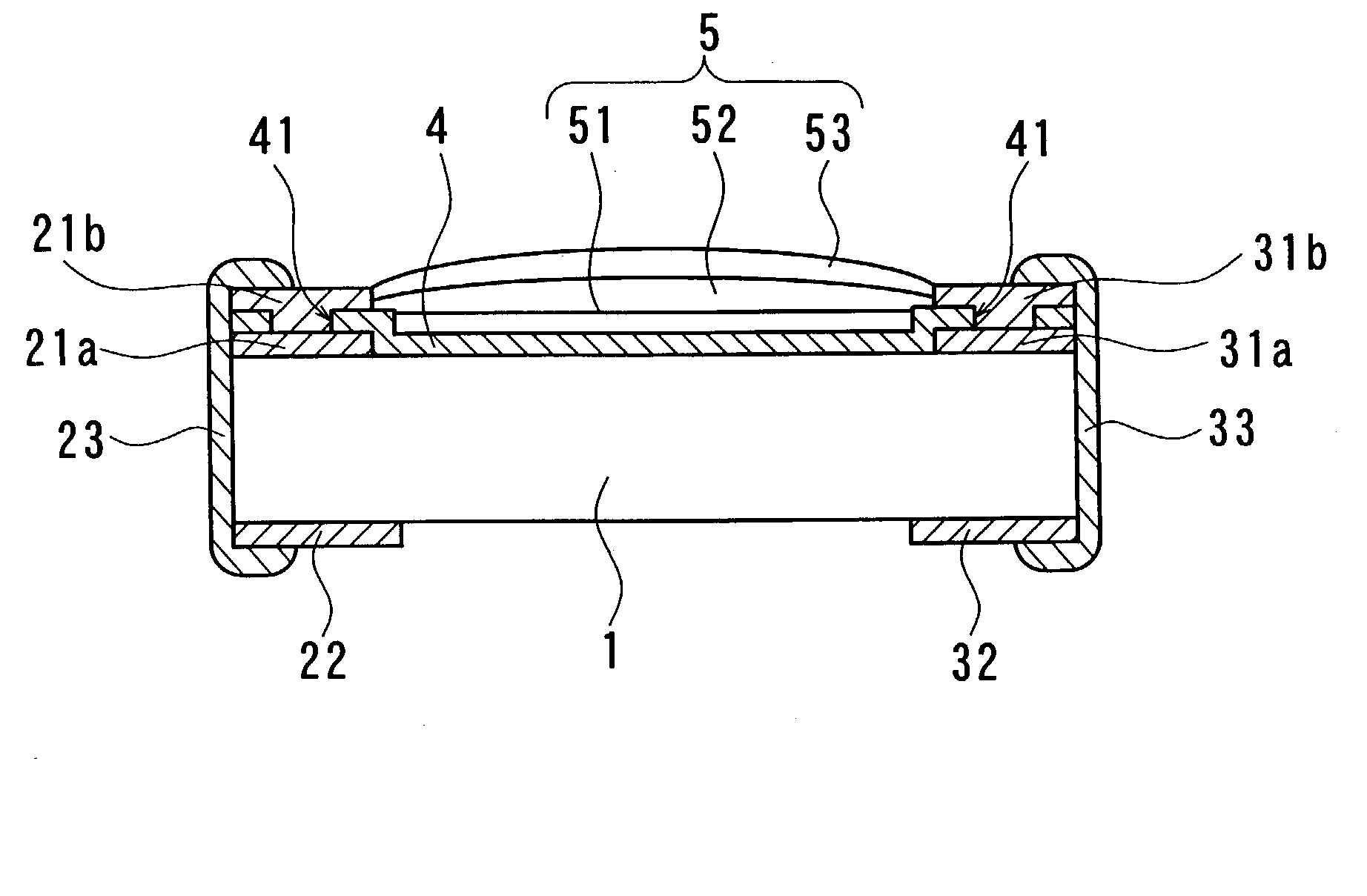
[0040] FIG. 4 shows a third embodiment of a chip resistor according to the invention, wherein in the case of adopting a composite body made up of a thin-film and a thick-film, and in particular, in the case of adopting a construction in which a thick-film is formed on top of a thin-film, means for enhancing tackiness between the thin-film and the thick-film formed thereon are provided.
[0041] That is, with the third embodiment shown in FIG. 4, upper surface electrodes 21, 31 are divided into first upper surface electrodes 21a, 31a and second upper surface electrodes 21b, 31b and a resistance 4 formed of the thin-film is sandwiched between the first upper surface electrodes 21a, 31a, formed of the thick film, and the second upper surface electrodes 21b, 31b, formed of the thick film as with the second embodiment, however, in this case, a through-hole 41 is provided in part of the resistance 4, on top of respective portions of the first upper surface electrodes 2...
PUM
 Abstract
Description
Claims
Application Information
 - R&D
- Intellectual Property
- Life Sciences
- Materials
- Tech Scout
- Unparalleled Data Quality
- Higher Quality Content
- 60% Fewer Hallucinations
Browse by: Latest US Patents, China's latest patents, Technical Efficacy Thesaurus, Application Domain, Technology Topic, Popular Technical Reports.
© 2025 PatSnap. All rights reserved.Legal|Privacy policy|Modern Slavery Act Transparency Statement|Sitemap|About US| Contact US: help@patsnap.com


