Systems and methods of in-situ digital eye characterization for serial data transmitter circuitry

a serial data transmitter and in-situ digital technology, applied in the field of serial data transmission, can solve the problems of external circuitry, transmission line and other external circuitry, and the reduction of repeatability of off-chip digital eye capture, so as to achieve accurate and repeatable capture and reduce repeatability

Active Publication Date: 2019-10-01
DELL PROD LP
View PDF16 Cites 0 Cited by
  • Summary
  • Abstract
  • Description
  • Claims
  • Application Information

AI Technical Summary

Benefits of technology

[0007]Disclosed herein are systems and methods that may be implemented in-situ and on-chip to capture a digital signal eye of a serial transmit signal produced by a transmitter circuit of integrated SerDes PHY circuitry, such as may be included in a storage device of an information handling system or in any other data communication architecture. In one embodiment, a serial transmit signal produced by a transmitter side circuit of a SerDes PHY transceiver circuit that is integrated on a single semiconductor integrated circuit chip may be looped back on-chip to the receiver side circuit of the same SerDes PHY transceiver circuit (e.g., looped back into the receiver analog front end (AFE)) such that an integrated digital eye monitor circuit of the SerDes receiver circuit may capture the digital eye of the serial transmit signal of the same SerDes PHY transceiver circuit rather than being transmitted off-chip to a serial transmit channel of a digital communication bus or other external communication media that is coupled to the SerDes PHY circuit. The integrated digital eye monitor circuit of the receiver side monitor circuit may be further configured to output the on-chip captured digital eye of the serial transmit signal, e.g., for display on a display device such as LCD or LED monitor. Because it is captured in-situ, on-chip and at the signal latch point, the digital eye of the serial transmit signal may be more accurately and repeatably captured using the disclosed systems and methods than is possible with a transmit signal digital eye that is captured by off-chip circuitry, such as test bench equipment (e.g., external oscilloscope coupled across an external digital communication path) where signal loss and / or interference degrades the digital eye accuracy. Such off-chip digital eye capture is subject to external errors and reduction in repeatability induced by transmission line and other external circuitry.
[0011]Advantages and capabilities that may be realized using embodiments of the disclosed systems and methods include, but are not limited to: accurate estimation of SerDes transmitter side settings with minimal signal distortion; testing and circuit characterization during SerDes PHY system operation in test mode without requiring special test cards, equipment and software for testing; real time capturing of data to help in fine tuning a particular SerDes circuit design for improved signal integrity (“SI”) margins; Volume qualification of SerDes circuitry with least scope for error; characterizing and / or screening of re-drivers and re-timers; data processing through external software that may be enabled through GPIO pins; and characterization of equalization and / or jitter components of transmitter side circuitry of a SerDes PHY transceiver. Moreover, in one embodiment using the disclosed systems and methods, transmitter side signal characteristics may identified, characterized and / or corrected for using the in-situ and on-chip captured digital signal eye of a serial transmit signal. Such signal characteristics include cross talk, loss, reflection, jitter, impedance, transmission line loss, voltage swing, rise time, transmitter process / voltage / temperature (PVT) variation.

Problems solved by technology

Such off-chip digital eye capture is subject to external errors and reduction in repeatability induced by transmission line and other external circuitry.

Method used


Image

  • Systems and methods of in-situ digital eye characterization for serial data transmitter circuitry
  • Systems and methods of in-situ digital eye characterization for serial data transmitter circuitry
  • Systems and methods of in-situ digital eye characterization for serial data transmitter circuitry

Examples


Embodiment Construction

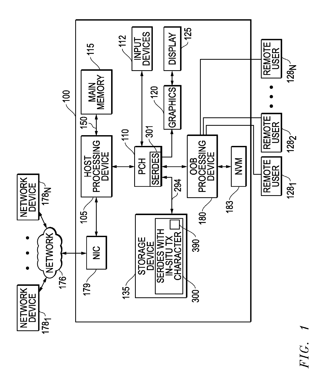
[0025]FIG. 1 illustrates one exemplary embodiment of an information handling system 100 configured as a server system that includes at least one host processing device 105 which may be a central processing unit (CPU) such as an Intel Pentium series processor, an Advanced Micro Devices (AMD) processor or other type of host processing device that executes an operating system (OS) for system 100. Host processing device 105 may be provided in one embodiment with an integrated memory controller (iMC) to facilitate memory functions, although it will be understood that a memory controller may be alternatively provided as a separate chip or other circuit in other embodiments. As shown in FIG. 1, main system memory 115 (e.g., DRAM) may be coupled via DDR channel 150 as shown to host processing device 105. An external display 125 (e.g., LCD or LED display, touchscreen, or other suitable display device) may be coupled to an optional discrete graphics processing unit (GPU) 120 to provide visual...


PUM


Abstract

Systems and methods are provided that may be implemented in-situ and on-chip to capture a digital signal eye of a serial transmit signal produced by a transmitter circuit of integrated SerDes PHY transceiver circuitry. In one example, a serial transmit signal produced by a transmitter side circuit of an integrated SerDes PHY transceiver circuit may be looped back on chip to the receiver side circuit of the same SerDes PHY transceiver circuit such that an integrated digital eye monitor circuit of the SerDes receiver circuit may capture the digital eye of the serial transmit signal of the same SerDes PHY circuit. In another example, a digital eye monitor circuit may be integrated on the transmitter side of an integrated SerDes PHY transceiver circuit such that a serial transmit signal produced by the transmitter side circuit of may be captured on-chip.

Description

FIELD OF THE INVENTION[0001]This invention relates generally to serial data transmission and, more particularly, to digital eye characterization for serial data transmitter circuitry.BACKGROUND OF THE INVENTION[0002]As the value and use of information continues to increase, individuals and businesses seek additional ways to process and store information. One option available to users is information handling systems. An information handling system generally processes, compiles, stores, and / or communicates information or data for business, personal, or other purposes thereby allowing users to take advantage of the value of the information. Because technology and information handling needs and requirements vary between different users or applications, information handling systems may also vary regarding what information is handled, how the information is handled, how much information is processed, stored, or communicated, and how quickly and efficiently the information may be processed...

Claims


Application Information

Patent Timeline
Patent Type & Authority Patents(United States)
IPC IPC(8): G06F13/40G06F13/42
CPCG06F13/4221G06F13/4282G06F13/4027G11C29/022
Inventor WALLACE, DOUGMUTNURY, BHYRAVKUMAR, VIJENDERA
Owner DELL PROD LP
Why Eureka
Try Eureka