Integration manufacturing method of cantilever beam type dot needle-point based on silicon oxide film

A silicon dioxide, cantilever beam technology, used in the manufacture of microstructure devices, processes for producing decorative surface effects, gaseous chemical plating, etc., can solve the problem of high processing and manufacturing costs, cantilever beam stress bending, bending deformation and other problems, to achieve the effect of convenient and reliable process flow, improved mechanical properties, and overall performance improvement.

Inactive Publication Date: 2006-02-08
SHANGHAI JIAO TONG UNIV
View PDF0 Cites 6 Cited by
  • Summary
  • Abstract
  • Description
  • Claims
  • Application Information

AI Technical Summary

Problems solved by technology

Hydrophilicity can be increased by depositing silicon oxide, but the added film may significantly change the stress characteristics of the cantilever, resulting in stress bending of the cantilever after release, and this longer cantilever is sensitive to the internal stress of the film structure The degree is quite high, and a little internal stress can lead to a large amount of bending deformation. In this way, the consistency of the tip of the high-order array cantilever beam faces severe challenges, because the inconsistent position of the array tip will cause it to lose its use value.
[0009] In addition, the cost of SOI silicon wafers is much higher than that of ordinary silicon wafers. The complexity of the above structure determines that it can only use dry back etching to realize the back hollow release operation, so its processing and manufacturing costs are relatively high

Method used


Image

  • Integration manufacturing method of cantilever beam type dot needle-point based on silicon oxide film

Examples


Embodiment 1

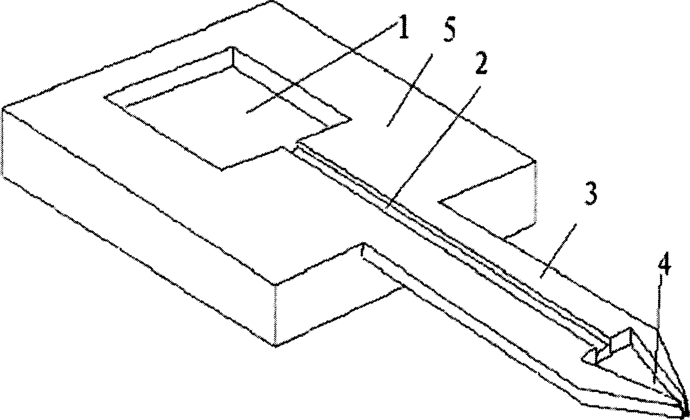
[0027] A 3-inch double-sided polished (100) silicon substrate 5 with a thickness between 500 microns was oxidized for 24 hours under standard wet oxidation process conditions to form a silicon dioxide film with a thickness of about 2.1 microns.

[0028] Then use a patterned positive resist with a thickness of 3 microns as a mask, and use a conventional reactive ion etching method to pattern the silicon dioxide film layer to form the overall outline pattern of the cantilever beam-type spotting needle tip, and the etching time is 65 minutes. The cantilever beam 3 is 800 microns in length and 120 microns in width, with a single tip that narrows at an inclination angle of 30°. At the same time, the thin slit structure of the tip 4 of the spotting needle point is etched, and the slit width is 2 microns, and at the same time, a silicon dioxide window for etching the liquid storage tank 1 is formed on the front side of the silicon substrate.

[0029] Then remove the glue, and use the...

Embodiment 2

[0034] The basic process flow is the same as in Example 1, except that the process parameters are changed, wherein the oxidation time of the single crystal silicon wafer is shortened to 15 hours, and the thickness of the corresponding oxide film is 1.7 microns. The size of the spotting needle tip remains unchanged, the etching time for forming the cantilever beam pattern is 55 minutes, and other parameters are unchanged, and the spotting needle tip can also be prepared, and the trial effect is basically the same as that of Example 1.

Embodiment 3

[0036] The basic process flow is the same as that of Example 1, except that the process parameters and structural parameters are changed, wherein the oxidation time of the single crystal silicon wafer is increased to 48 hours, and the thickness of the corresponding oxide film is 2.5 microns. The individual size of the spotting needle tip is adjusted to a length of 1000 microns and a width of 200 microns. The tip still adopts a slit structure with a design size of 1.5 microns. A group of 6 forms an array, and the distance between individuals is 200 microns to form the etching of the cantilever beam pattern. The time is 90 minutes, and other parameters are kept constant, and the spotting needle tip array can be prepared, which can meet the requirements of commercial sample spotting equipment after trial use, and the spotting efficiency is significantly improved.


PUM

PropertyMeasurementUnit
lengthaaaaaaaaaa
widthaaaaaaaaaa
thicknessaaaaaaaaaa

Abstract

A integration Manufacturing method for cantilever beam type spot needlepoint base on silica dioxide film. First growing a layer silica dioxide film by thermal oxidation on the surface of a double-faced mirror polish silicon basal body, then opening a liquid storage groove window on the oxidation film and forming a fluid passage anf forming a fine structure patterns of the cantilever beam and the needle point by two photo resist mask reaction ion etching art work, and then open a window for back etching monocrystalline silicon releasing the cantilever beam on the back side of the silicon in mask chemical etching, using KOH solution aeolotropism masking, getting rid of the silicon basal body under the cantilever beam, releasing the silica dioxide cantilever beam needle point which has been micro machine-shaping. The invention uses thermal oxidation thermal oxidation film replacing general monocrystalline silicon film as constructional material for making cantilever beam type spot needle point, and not only can improve the hydrophilicity of the needle point and the fluid channel, have no inner stress, but also get a convenience and highly effective integration manufacturing process flow.

Description

technical field [0001] The invention relates to a method for manufacturing a needle point required for sample preparation of a biochip, in particular to an integrated manufacturing method for a cantilever beam type sample point needle point based on a silicon dioxide film, which belongs to the field of microfabrication technology and is also a biochip technology category. Background technique [0002] The core of biochip manufacturing is lattice preparation technology. Affymetrix, which has registered the Genechip trademark, has a patented technology for photodeprotection in situ synthesis of biochips, making it a leader in this field, but this method also has low-level Due to problems such as high array cost and high synthesis error rate, its gene chips are currently mainly used in the field of scientific research, and other companies are more likely to use spotting methods to prepare gene chips. [0003] Generally speaking, the sample size of sample preparation is larger ...

Claims


Application Information

Patent Timeline
Patent Type & Authority Applications(China)
IPC IPC(8): B81C1/00
Inventor 丁桂甫姚锦元
Owner SHANGHAI JIAO TONG UNIV
Why Eureka
Try Eureka