A method for corroding sapphire graphic substrate by wet-process
A wet etching, patterned substrate technology, applied in lasers, electrical components, climate sustainability, etc., can solve the problems of limiting crystal quality, easy introduction of impurities, increasing stress, etc., to enhance radiation recombination, reduce costs, reduce The effect of small density
- Summary
- Abstract
- Description
- Claims
- Application Information
AI Technical Summary
Problems solved by technology
Method used
Image
Examples
Embodiment 1
[0023] Embodiment 1, preparation sapphire pattern substrate 1
[0024] Using plasma-enhanced chemical vapor deposition (PECVD), a silicon dioxide mask layer with a thickness of 500nm is evaporated on the C-plane sapphire;
[0025] Utilize photolithography technology to photoetch a striped silicon dioxide mask pattern along the [11 20] direction on the C-plane sapphire on which the silicon dioxide mask layer has been evaporated, and the length of the silicon dioxide mask layer stripe pattern is 50mm, the width is 1μm, the width of the window area is 1μm, and the length is 50mm.
[0026] The substrate was put into an etching solution mixed with sulfuric acid and phosphoric acid with a volume ratio of 10:1, heated in a temperature-controlled furnace, etched at 200°C for 2 hours, taken out, rinsed with deionized water, and obtained The resulting substrate with a mesa height of 0.5 μm was etched.
[0027] Finally, the wet-etched substrate was put into a hydrofluoric acid solution...
Embodiment 2
[0031] Embodiment 2, preparation sapphire pattern substrate II
[0032] Using a method similar to that of Example 1, prepare a stripe pattern along the [1 100] direction on the C-plane sapphire, wherein the length of the stripe pattern on the silicon dioxide mask layer is 1 mm, the width is 0.1 μm, and the width of the window area is 0.2 μm . After wet etching with sulfuric acid solution at 600°C for 0.5 hours, the obtained sapphire pattern substrate II is as follows figure 2 As shown, the width of the mesa is 0.1 μm, the length is 1 mm, and the height is 3 μm; the width of the groove is 0.1 μm, and the length of the groove is 1 mm; the adjacent sides of the groove-like stripes are asymmetric planes.
Embodiment 3~7
[0033] Embodiment 3~7, prepare sapphire pattern substrate III~VII
[0034] According to the method of Example 1, sapphire pattern substrates III-VII with different patterns were prepared, which are listed in Table 1.
[0035] Reality
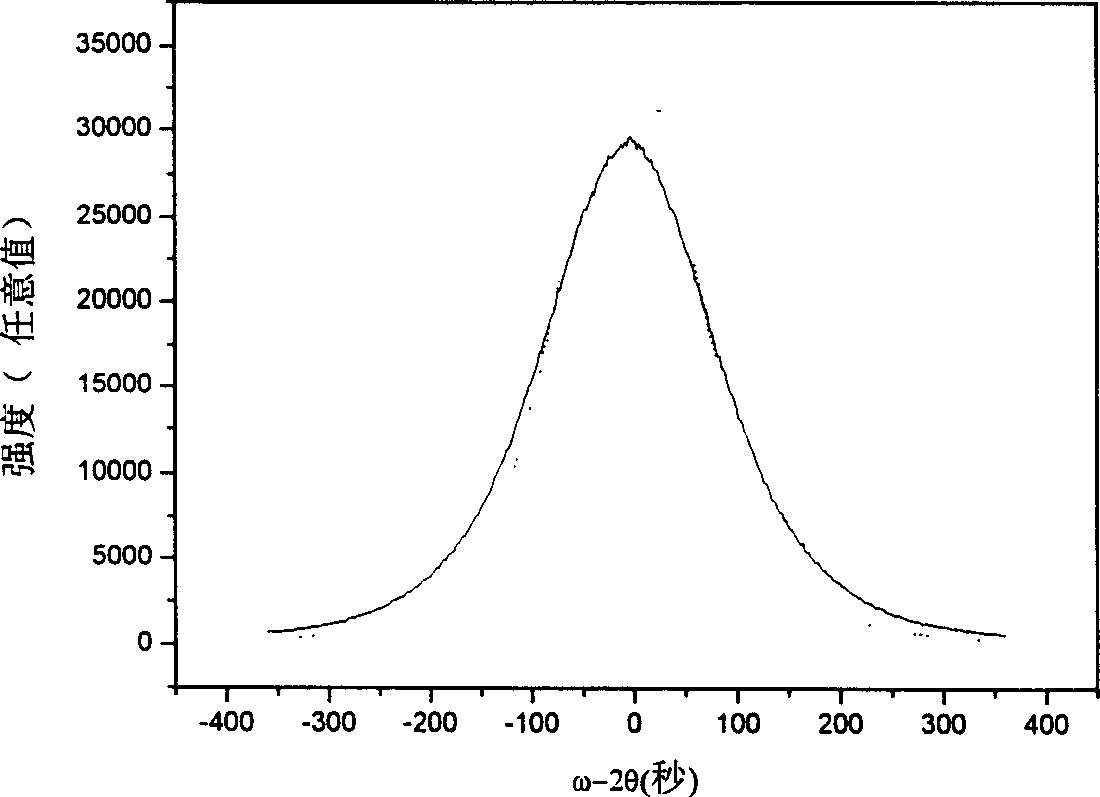
[0036] Compared with the GaN material grown on common substrates, the GaN material grown epitaxially on the pattern substrates II-VII provided by the present invention has a smaller half-width of the diffraction peak of the (002) plane in its X-ray diffraction spectrum, And in the photoluminescence spectrum, the luminescence peak caused by defects or impurities near 550 nanometers is suppressed, which shows that the graphic substrate provided by the invention improves the crystal quality.
PUM
 Abstract
Description
Claims
Application Information
 - R&D
- Intellectual Property
- Life Sciences
- Materials
- Tech Scout
- Unparalleled Data Quality
- Higher Quality Content
- 60% Fewer Hallucinations
Browse by: Latest US Patents, China's latest patents, Technical Efficacy Thesaurus, Application Domain, Technology Topic, Popular Technical Reports.
© 2025 PatSnap. All rights reserved.Legal|Privacy policy|Modern Slavery Act Transparency Statement|Sitemap|About US| Contact US: help@patsnap.com


