
Electroplating pretreatment solution and electroplating pretreatment method

A pretreatment, solution technology, applied in secondary treatment of printed circuits, removal of conductive materials by chemical/electrolytic methods, circuits, etc., can solve problems such as reducing insulation resistance, difficulty in removing nickel and chromium, and residues

Inactive Publication Date: 2004-10-20
MITSUI MINING & SMELTING CO LTD
View PDF0 Cites 0 Cited by
  • Summary
  • Abstract
  • Description
  • Claims
  • Application Information

AI Technical Summary

Problems solved by technology

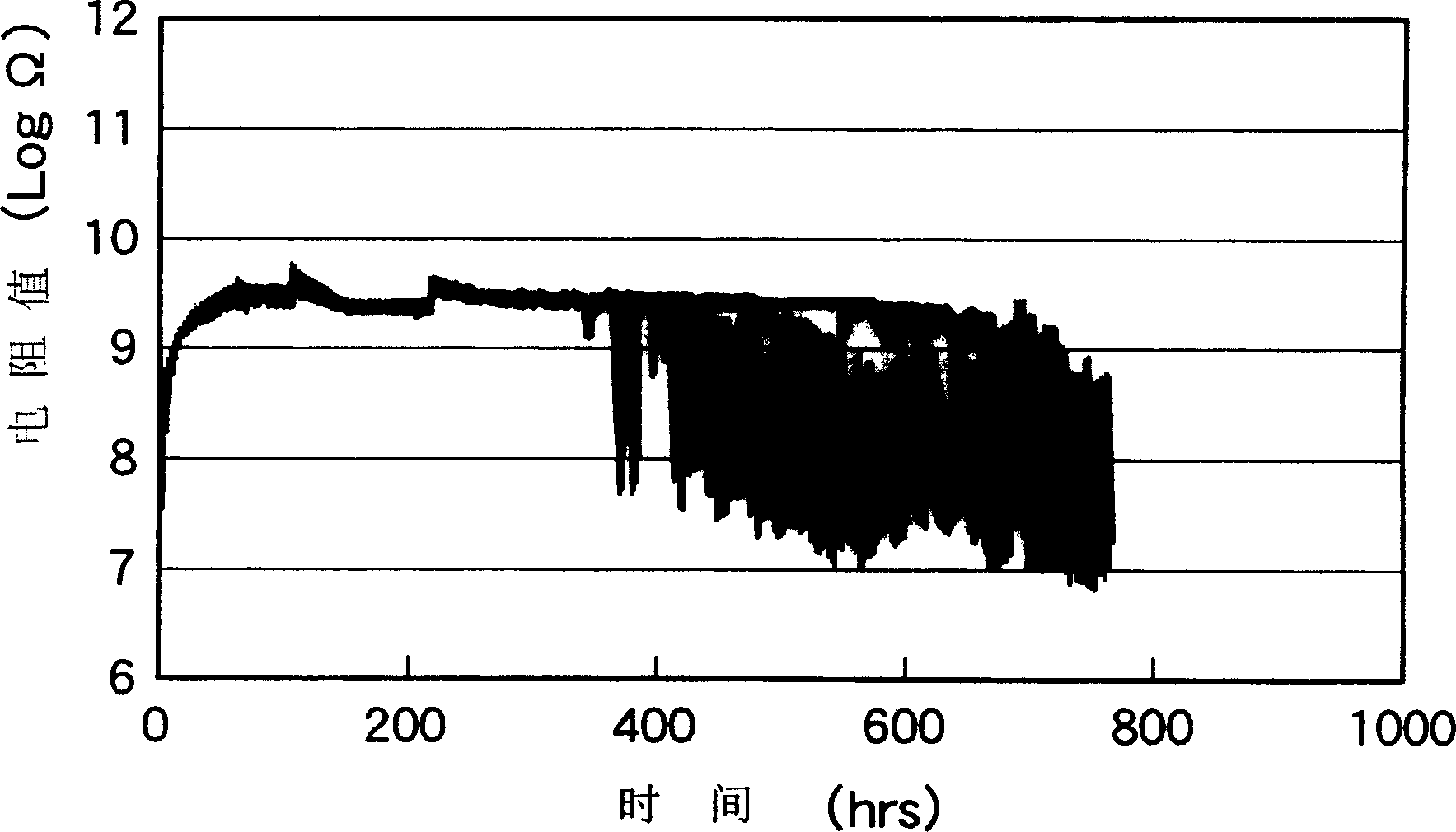
However, if a DC voltage is continuously applied to the wiring pattern treated by this method and electroless tin-plated under the conditions of constant temperature and constant humidity (such as 85°C x 85% RH x DC60V), then in about 100~ After 200 hours, burning may occur between the wires of the wiring pattern, and in addition, copper branches may appear to significantly reduce the insulation resistance
That is, by using only K 2 S 2 o 8 +H 2 SO 4 or H 2 o 2 Conventional electroplating pretreatment solution, although copper can be etched, but nickel and chromium are difficult to remove, therefore, nickel and chromium often remain between the wiring
[0011] In addition, when treating with a commercially available solution for dissolving nickel, insufficient cleaning can cause the treated substance to remain on the wiring pattern and have a more detrimental effect on the insulation characteristics

Method used


Image

  • Electroplating pretreatment solution and electroplating pretreatment method
  • Electroplating pretreatment solution and electroplating pretreatment method
  • Electroplating pretreatment solution and electroplating pretreatment method

Examples


Embodiment 1

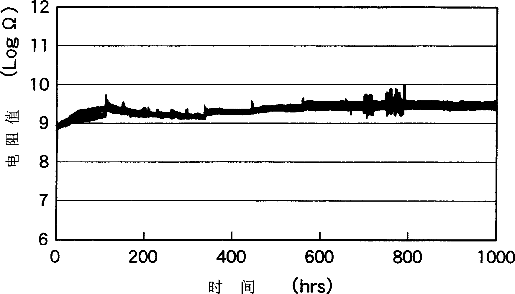
[0061]Containing the cationic surfactant (dodecyl) of the phenolsulfonic acid of 160g / L water, the thiourea of ​​160g / L water, the fluoboric acid of 60g / L water, the hypophosphorous acid of 60g / L water and 20g / L water Trimethylammonium chloride) electroplating pretreatment solution was prepared. The pH value of the electroplating pretreatment solution shall not exceed 1 at 25°C.

[0062] S'PER FLEX (trade name, supplied by Sumitomo Metal Mining Co., Ltd.) was sputtered with a Ni-Cr alloy layer with a thickness of 70 Å containing 7% by weight of Cr and 9.3% by weight of Ni , and then the alloy layer was plated with copper by electroless plating, and further prepared by plating copper with a thickness of 8 μm by electroplating. The S’PER FLEX is covered with photoresist, then the photoresist is exposed and alkaline developed, then, using copper chloride solution, formed by etching such as figure 1 Comb-patterned electrodes with a line pitch of 50 μm are shown, thereby preparin...

Embodiment 2

[0072] A test piece was prepared in the same manner as in Example 1, except that the line pitch of the comb-shaped pattern electrodes was changed to 30 μm.

[0073] The resistance of the obtained three test pieces was measured in the same manner as in Example 1. As a result, no decrease in insulation resistance was observed in the three test pieces even after 1000 hours had elapsed.


PUM

PropertyMeasurementUnit
thicknessaaaaaaaaaa

Abstract

A plating-pretreatment solution comprising an organic sulfonic acid, thiourea, fluoroboric acid and hypophosphorous acid and a plating-pretreatment method comprising contacting a film carrier tape in which a wiring pattern is formed on a surface of an insulating film with a plating-pretreatment solution comprising an organic sulfonic acid, thiourea, fluoroboric acid and hypophosphorous acid to remove metals remaining on the insulating film. According to the plating-pretreatment solution and the plating-pretreatment method, metals remaining on the surface of the insulating film exposed by etching are removed, and the occurrence of migration is prevented.

Description

technical field [0001] The invention relates to an electroplating pretreatment solution and a method for using the solution. More specifically, the present invention relates to a solution for removing metal remaining on the surface of an insulating film between wires of a wiring pattern in a strip having a metal layer on the surface of the insulating film etched by a fine line pitch, and a method of use thereof. It is used after the wiring pattern is formed and before the wiring pattern is plated. Background technique [0002] Electronic parts are conventionally mounted with a film carrier tape. Film carrier tapes for mounting electronic parts are produced by bonding a conductive metal foil such as copper foil to the surface of an insulating film such as a polyimide film through an adhesive layer, coating the conductive metal foil with a photoresist The surface of the metal foil, expose and develop the photoresist to form the desired pattern, use the obtained pattern as a ...

Claims


Application Information

Patent Timeline
Patent Type & Authority Applications(China)
IPC IPC(8): C25D5/34C23C18/18C23F1/16H01L21/48H01L21/60H05K3/26
CPCH05K2201/0761H05K3/26H01L21/4846C23C18/1844H05K2203/0789C23C18/1608C23C18/18H01L24/06C25D5/34
Inventor 片冈龙男明石芳一
Owner MITSUI MINING & SMELTING CO LTD
Learn More