Semiconductor film and producing method and equipment, and method for producing single crystal film
A single crystal thin film, semiconductor technology, applied in the field of semiconductor thin film, thin film transistor semiconductor thin film and its production, can solve problems such as deformation and productivity decline
- Summary
- Abstract
- Description
- Claims
- Application Information
AI Technical Summary
Problems solved by technology
Method used
Image

Examples
no. 1 Embodiment
[0068] A method for producing a single-crystal thin film according to the present invention includes the step of forming a non-single-crystal thin film on an insulating substrate, subjecting the non-single-crystal thin film to a first heat treatment, thereby forming a polycrystalline film in which polycrystalline grains are arranged in an approximately regular pattern The step of polycrystalline film, and the step of performing the second heat treatment on the polycrystalline film to make the polycrystalline grains combine with each other, thus forming the single crystal film.
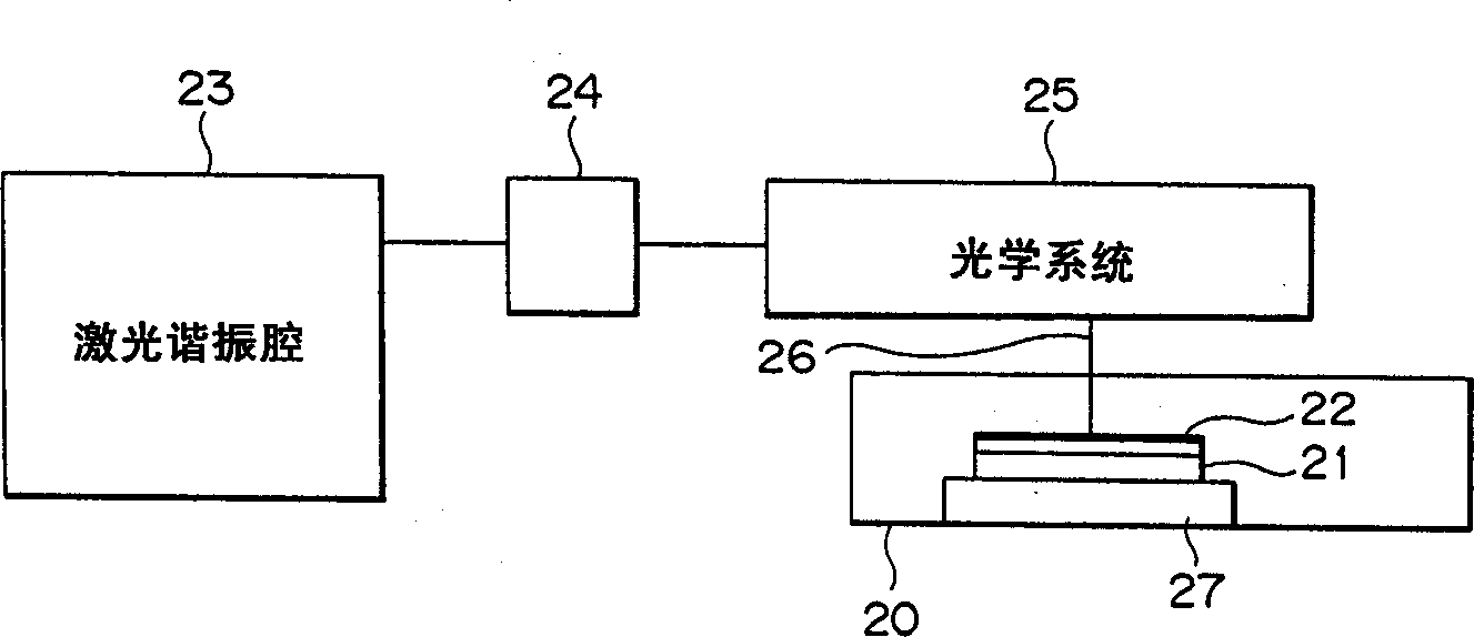
[0069] According to the method for producing single crystal thin film of the present invention, refer to Figure 1-6 will be described below. figure 1An example of an excimer laser irradiation apparatus used in the method of producing a semiconductor thin film as a single crystal thin film according to the present invention is shown. First, an excimer laser irradiation apparatus for irradiating a semi...
no. 2 Embodiment
[0087] An active matrix type display as an example of a semiconductor device using a thin film transistor produced by the method for producing a single crystal thin film according to the present invention will be referred to Figure 7 described below. In this embodiment, a semiconductor device is formed by using a thin film having micro-protrusions as a channel. see Figure 7 , the display has a panel structure including a pair of insulating substrates 51 and 52, and an electro-optical material 53 fixed therebetween. For example, a liquid crystal material is used as the electro-optical material 53 . The pixel array portion 54 and the synchronization circuit portion are collectively formed on the lower insulating substrate 51 . The synchronous circuit portion is divided into a vertical scanner 55 and a horizontal scanner 56, and a terminal portion 57 for external connection is formed at the upper end of the peripheral portion of the insulating substrate 51. The terminal par...
no. 3 Embodiment
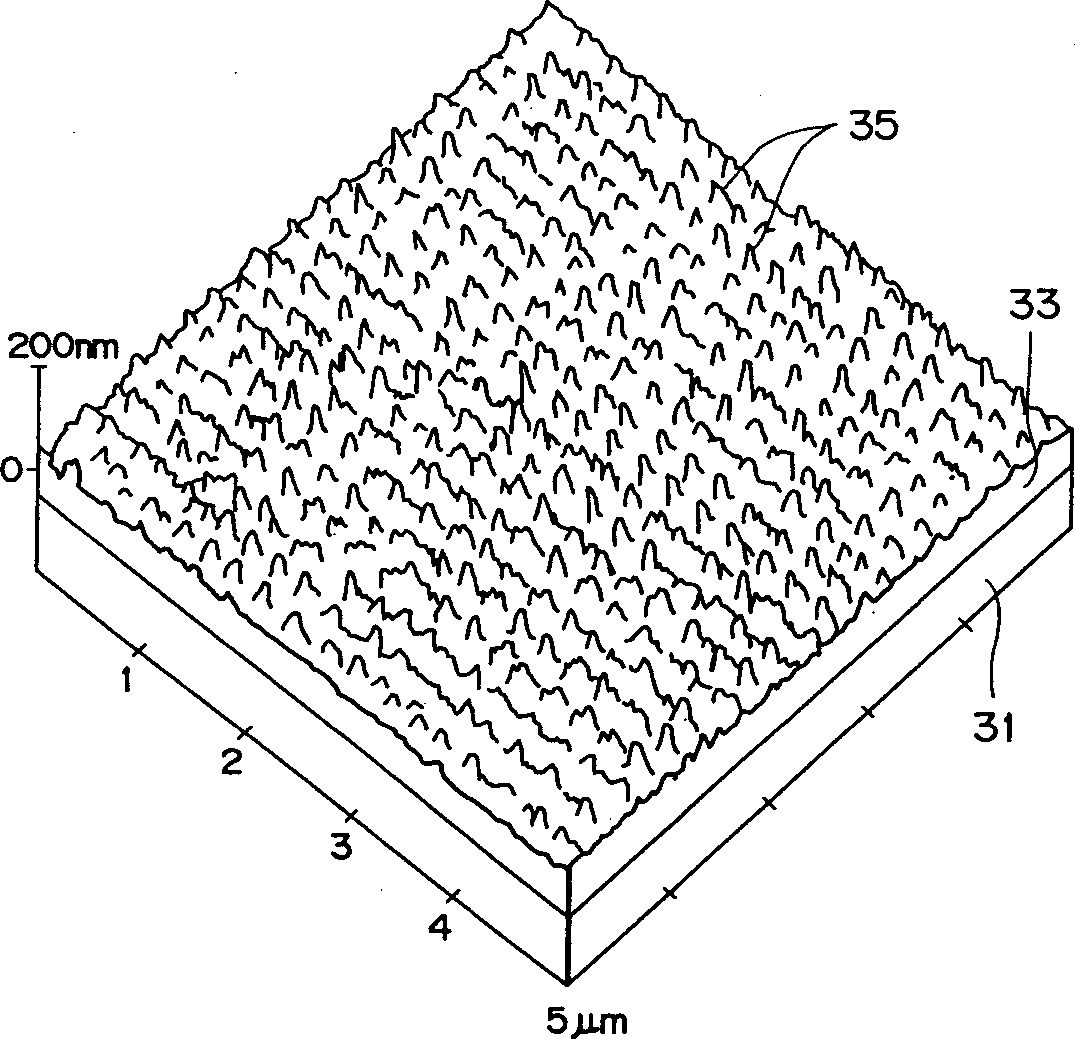
[0090] The semiconductor film in this embodiment is shaped as a semiconductor film formed on an insulating substrate, wherein micro-protrusions are formed on the surface of the semiconductor film.
[0091] The semiconductor thin film in this embodiment is also formed as a semiconductor thin film formed on an insulating substrate by a polycrystalline thin film in which polycrystalline grains are arranged in an approximately regular pattern, wherein each microprotrusion is formed on at least 3 or more Boundary locations between grains.
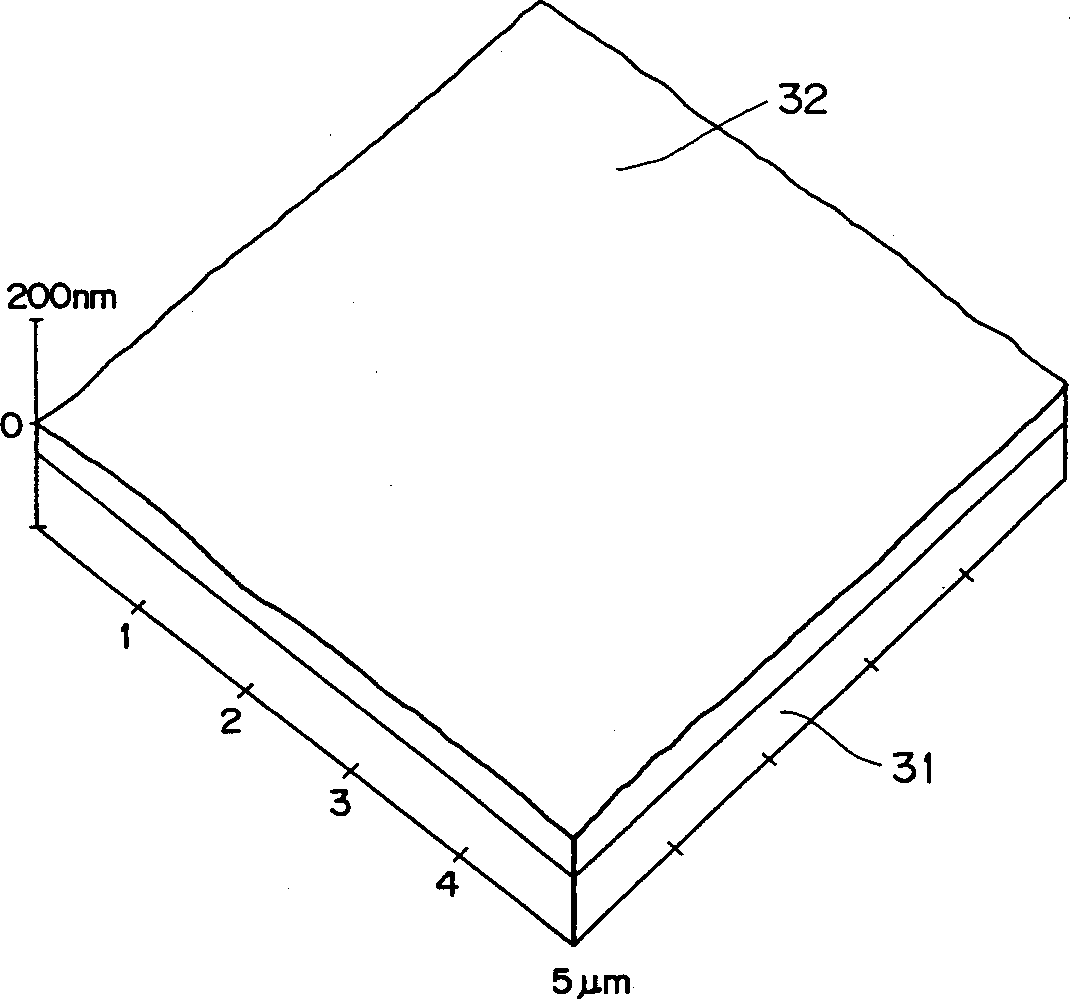
[0092] Figure 8 is a schematic diagram of a semiconductor thin film according to the present invention. see Figure 8 A crystallized thin film 102 is formed on an insulating substrate 101 as an insulating substrate, and a large number of microprotrusions 103 are formed on the surface of the crystallized thin film 102 .
[0093] As the insulating substrate 101, there may be various substrates such as glass substrates having specific rigidity ...
PUM
| Property | Measurement | Unit |
|---|---|---|
| Thickness | aaaaa | aaaaa |
| Height | aaaaa | aaaaa |
| Diameter | aaaaa | aaaaa |
Abstract
Description
Claims
Application Information
 - R&D
- Intellectual Property
- Life Sciences
- Materials
- Tech Scout
- Unparalleled Data Quality
- Higher Quality Content
- 60% Fewer Hallucinations
Browse by: Latest US Patents, China's latest patents, Technical Efficacy Thesaurus, Application Domain, Technology Topic, Popular Technical Reports.
© 2025 PatSnap. All rights reserved.Legal|Privacy policy|Modern Slavery Act Transparency Statement|Sitemap|About US| Contact US: help@patsnap.com