Multilayer printed wiring board and its manufacturing method, and resin composition for filling through-hole

A technology for printed circuit boards, conductive compositions, applied in the direction of multi-layer circuit manufacturing, printed circuit manufacturing, printed circuits, etc., can solve gaps or voids, lack of adhesion of conductive materials, and insufficient use of high-density wiring functions, etc. question

Inactive Publication Date: 2000-11-01
IBIDEN CO LTD
View PDF1 Cites 14 Cited by
  • Summary
  • Abstract
  • Description
  • Claims
  • Application Information

AI Technical Summary

Problems solved by technology

[0013] ④. In printed wiring boards of the type described in Japanese Unexamined Patent Publication 4-92496, gaps or voids tend to form due to lack of sufficient adhesion between the conductor layer and the conductive material in the through hole
[0018] ⑥. The technology disclosed in Japanese Unexamined Patent Publication 5-243728 does not involve laminated multilayer printed circuit board technology, and therefore, does not make full use of the inherent high-density wiring function in this laminated method

Method used


Image

  • Multilayer printed wiring board and its manufacturing method, and resin composition for filling through-hole
  • Multilayer printed wiring board and its manufacturing method, and resin composition for filling through-hole
  • Multilayer printed wiring board and its manufacturing method, and resin composition for filling through-hole

Examples


Embodiment 1

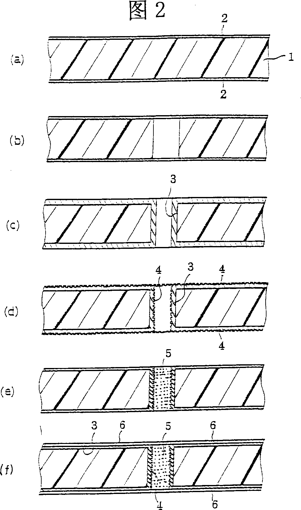
[0177] (1), a copper-clad laminate made of 0.8 mm thick polytetrafluoroethylene resin (hereinafter referred to as trade name: Teflon) substrate 1 and 18 microns thick, copper foil 2 laminated on the substrate 1 ( Matsushita Electric Works, Ltd., manufactured, trade name: R4737) as a raw material, the surface of the copper foil 2 is roughened (see FIG. 2(a)). Drill holes on the copper-clad laminate first, and then treat the inner surface of the hole with a modifier containing organic metal sodium (manufactured by Junkosha Co. Ltd., product name Tetraetch) to improve the wettability of the hole surface (see Figure 2 ( b)).

[0178] Then coat palladium-tin colloid on the substrate, then immerse the substrate in the electroless plating solution comprising the following composition to form a 2 micron thick electroless plating film on the entire substrate surface:

[0179] [Chemical Plating Solution]

[0180] EDTA 150 g / l

[0181] Copper Sulfate 20 g / L

[0182] Forma...

Embodiment 2

[0221] (Example 2) Multilayer core substrate

[0222] (1) Form an etch-resistant layer on both surfaces of a double-sided copper-clad laminate 1' with a thickness of 0.5 mm, then etch with an aqueous solution of sulfuric acid and hydrogen peroxide to obtain a substrate with a conductor circuit, and then place the Glass fiber-epoxy resin prepreg and copper foil 2 at a temperature of 165-170°C and a pressure of 20 kg / cm 2 Laminated successively on both surfaces of the substrate under the conditions to form a multilayer core substrate 1' (see Figure 5 (a)).

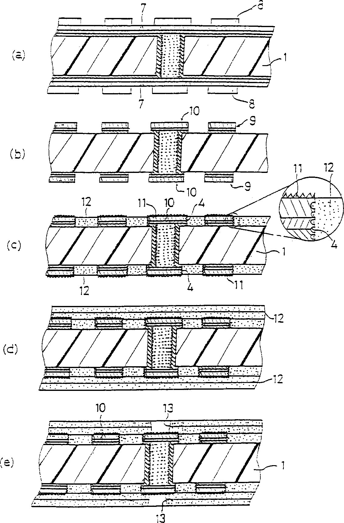
[0223] (2), drilling a diameter on the multilayer core substrate 1 ' is a through hole with a diameter of 300 microns (see Figure 5 (b)), then coated with palladium-tin colloid, then the substrate is immersed in the composition of the same chemical plating solution as in Example 1 to form a 2 micron thick chemical plating film on the entire substrate surface. Then make this substrate carry out electroplating copper plat...

Embodiment 3

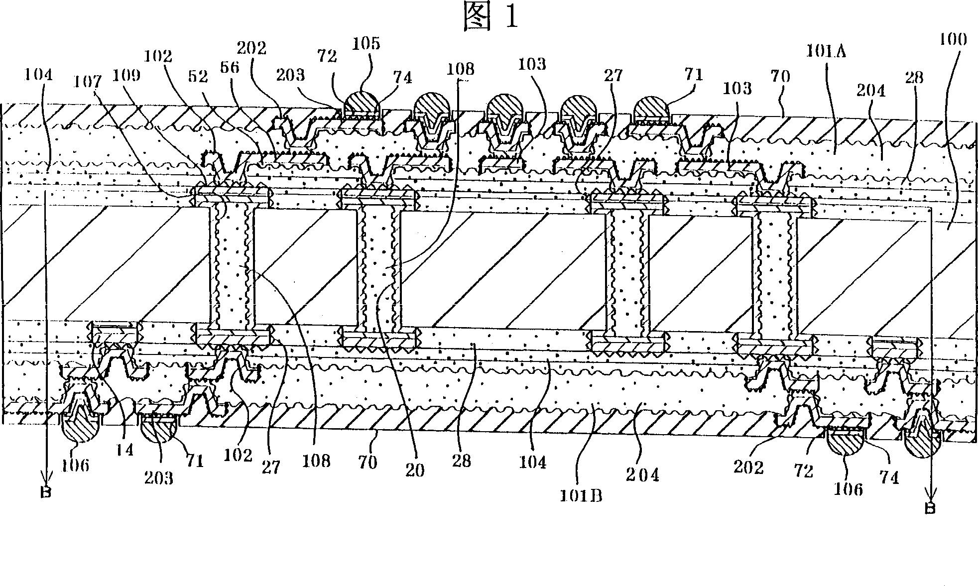
[0252] A multilayer printed wiring board was fabricated in the same manner as in Example 1, except that when the through hole was filled with copper paste, the conductor layer 10 covering the through hole was not formed to cover the exposed copper paste. According to the present method, since the surface of the copper paste can be easily removed when the hole is formed in the insulating resin layer by the laser beam irradiation method, pits may be formed.


PUM


Abstract

A multilayer printed wiring board is composed of a substrate (100) provided with through-holes (107), and a wiring board (101) formed on the substrate (100) through the interposition of an interlaminar insulating resin layer (104), the through-holes (107) having a roughened internal surface and being filled with a filler (108), an exposed part of the filler (108) in the through-holes (107) being covered with a through-hole-covering conductor layer (109), and a viahole (102) formed just thereabove being connected to the through-hole-covering conductor layer (109). Without peeling between the through-holes (107) and the filler (108), this wiring board has a satisfactory connection reliability between the through-holes (107) and the internal layer circuit (103) and provides a high density wiring.

Description

technical field [0001] The present invention relates to a multilayer printed wiring board for packaging boards for mounting integrated circuit (IC) chips, etc., and a method of manufacturing the same. In particular, the present invention relates to a multilayer printed wiring board capable of easily forming high wiring density and capable of preventing through-holes or the like when subjected to heat cycles, for example, Multilayer printed wiring boards with cracks or the like in adjacent parts. [0002] The present invention also relates to a resist composition for filling through-holes in multilayer printed wiring boards, which can maintain the contact between the via hole and the through-hole even under high temperature, high humidity conditions or conditions that cause thermal cycling. Good electrical connection. technical background [0003] Generally speaking, through holes are used for electrical connection between the front and back of the double-sided multilayer pr...

Claims


Application Information

Patent Timeline
Patent Type & Authority Applications(China)
IPC IPC(8): H05K3/00H05K3/38H05K3/46
CPCH05K3/4602H05K3/383Y10S428/901H05K3/4069H05K2201/0209H05K2201/09563H05K3/0094H05K2201/0959H05K2201/0347H05K2201/0212H05K3/384H05K2201/09536H05K2201/0257H05K2201/0215H05K3/385H05K2201/096Y10T428/24917B32B3/00
Inventor 浅井元雄岛田宪一野田宏太苅谷隆濑川博史
Owner IBIDEN CO LTD
Why Eureka
Try Eureka