Silicon-aluminium-silicon structure micro machinery processing method of full dry method

A technology of micromachining and silicon structure, applied in microstructure technology, microstructure device, manufacturing microstructure device, etc., can solve the problems of reduced processing yield, complicated manufacturing process, high temperature treatment, etc., and achieves low manufacturing cost and operation. Simple process and low equipment requirements

Inactive Publication Date: 2005-11-16
THE 13TH RES INST OF CHINA ELECTRONICS TECH GRP CORP
View PDF0 Cites 0 Cited by
  • Summary
  • Abstract
  • Description
  • Claims
  • Application Information

AI Technical Summary

Problems solved by technology

In the silicon-based process, the surface processing adopts a multi-layer thin film structure (generally less than 3 μm) and sacrificial layer corrosion technology. The production process is complicated and difficult to control. At present, there are few domestic applications. The bulk silicon process is mainly used, and the bulk silicon process is used most. The most important is the bulk silicon melting process, that is, the double-layer structure of silicon-glass bonding. Compared with the surface process, the bulk silicon process has a larger processing space (generally greater than 20 μm), but the traditional bulk silicon melting process requires a long time and high temperature. Diffusion of concentrated boron, which will bring greater stress to the device and cause structural deformation and performance degradation of the device. In addition, the traditional bulk silicon melting process requires special equipment to thin and polish the chip, which will make the processing The yield rate is greatly reduced, and the traditional bulk silicon melting process also requires a toxic wet etching process that is harmful to humans, so the traditional bulk silicon melting process has many shortcomings
In order to overcome these shortcomings, the SOI (silicon-oxide layer-conductive layer structure) process was invented later. This process makes the shortcomings of stress, small longitudinal dimension and poor consistency in micromachining well resolved, but SOI There are also deficiencies in the technology, such as strict requirements on the purification environment and high temperature treatment during production

Method used


Image

  • Silicon-aluminium-silicon structure micro machinery processing method of full dry method
  • Silicon-aluminium-silicon structure micro machinery processing method of full dry method
  • Silicon-aluminium-silicon structure micro machinery processing method of full dry method

Examples


Embodiment Construction

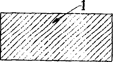
[0024] (1) Adopt commercially available general-purpose double-sided polished P-type single crystal silicon wafer 1 and double-sided polished N-type single crystal silicon wafer 2, both of which have a thickness of 280 μm to 320 μm, and the thickness of the embodiments is 300 μm, such as Picture 1-1 , 1-2.

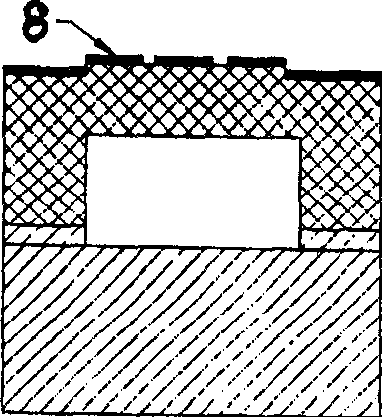
[0025] (2) Coating a layer of positive AZ1450 type photoresist 3 on the front side of the N-type monocrystalline silicon wafer 2, the thickness of the photoresist 3 is 2 μm, such as Figure 1-3 .

[0026] (3) photoresist 3 is carried out to the photoresist 3 on the front side of the N-type single crystal silicon wafer 2 with a commercially available general-purpose photolithography machine, and the pattern window of the alignment mark 4 of the microstructure 9 is formed on the front side of the N-type single crystal silicon wafer 2, Such as Figure 1-4 .

[0027] (4) Using the photoresist 3 as a mask, use a general reactive ion etching machine to etch the silicon on th...


PUM

PropertyMeasurementUnit
thicknessaaaaaaaaaa
depthaaaaaaaaaa
thicknessaaaaaaaaaa

Abstract

The present invention discloses fully dry process of making micro machine in Si-Al-Si structure, and relates to the manufacture of device for microelectronic mechanical system. The technological process including double-side photoetching, deep reaction ion etching and Si-Al-Si linking is adopted to realize manufacture of movable suspension structure with low stress and great longitudinal size and reaching the aims of optimizing micro machine making process, lowing cost, simplifying and raising product quality. The present invention is suitable for the manufacture of optical switch, capacitive micro acceleration meter, variable light attenuator and other movable micro structure devices.

Description

technical field [0001] The invention relates to an all-dry silicon-aluminum-silicon structure micromachining method in the technical field of microelectronic machining, and is especially suitable for various movable microelectronic mechanical structures with low stress, smooth surface and large longitudinal dimension device fabrication. Background technique [0002] Micro-electro-mechanical system, also known as MEMS, refers to a controllable and movable micro-electromechanical device with a size below the millimeter level. The combination of these constitutes a system with specific functions, which has the advantages of light weight, small size, low cost and integration. MEMS can not only integrate sensors, actuators and digital circuits on a semiconductor chip to realize the integration of the whole system, but also manufacture sensors, actuators and circuits separately and then mix and integrate them. The main application fields of MEMS are: guidance, navigation, micro-...

Claims


Application Information

Patent Timeline
Patent Type & Authority Patents(China)
IPC IPC(8): B81C1/00
Inventor 徐永青
Owner THE 13TH RES INST OF CHINA ELECTRONICS TECH GRP CORP
Why Eureka
Try Eureka