Method for regulating and controlling built electric field in active region of deep ultraviolet light emitting diode

A technology of light-emitting diodes and built-in electric fields, applied in circuits, electrical components, sustainable manufacturing/processing, etc., can solve problems such as high efficiency, easy leakage, and the impact of electronic effective barrier heights

Pending Publication Date: 2022-08-09
SHANDONG UNIV
View PDF2 Cites 2 Cited by
  • Summary
  • Abstract
  • Description
  • Claims
  • Application Information

AI Technical Summary

Problems solved by technology

However, the research of the present invention is based on InGaN-based quantum wells. For deep ultraviolet light-emitting diodes, due to the strong electron injection ability, the PN double doping close together will cause the effective barrier height of electrons to be affected, thereby Easier to leak into the P-type zone
At the same time, the weakened electric field in the quantum barrier cannot be efficiently applied to the quantum well, and the quantum well is the main area where electrons and holes recombine

Method used


Image

  • Method for regulating and controlling built electric field in active region of deep ultraviolet light emitting diode
  • Method for regulating and controlling built electric field in active region of deep ultraviolet light emitting diode
  • Method for regulating and controlling built electric field in active region of deep ultraviolet light emitting diode

Examples


Embodiment 1

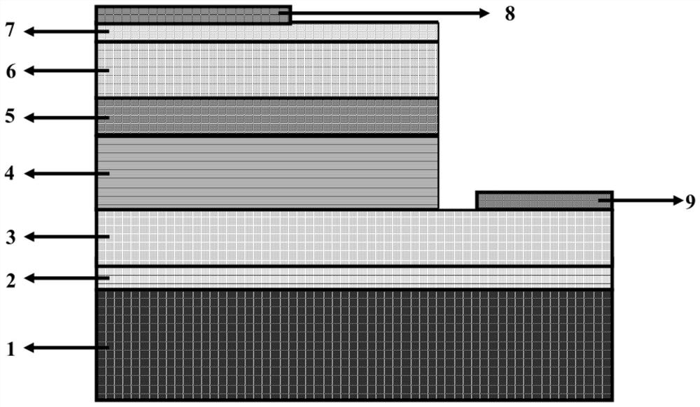
[0054] figure 1 , figure 2 and image 3 This is a schematic structural diagram of an AlGaN-based deep ultraviolet light emitting diode with n-type and p-type doped quantum barrier structures proposed by the present invention.

[0055] A method for regulating and controlling the electric field built in the active region of a deep ultraviolet light emitting diode, the deep ultraviolet light emitting diode comprises a substrate 1, a buffer layer 2, an n-type semiconductor electron injection layer 3, and a multi-quantum well active layer in order from bottom to top 4. The p-type electron blocking layer 5, the p-type semiconductor hole injection layer 6, the p-type contact layer 7, the p-type electrode 8, and the n-type electrode 9 are provided on the other side of the n-type semiconductor electron injection layer.

[0056] In the above structure, the material of the substrate 1 is a SiC substrate, the material of the buffer layer 2 is AlN, the thickness is 200 nm, and the mater...

Embodiment 2

[0070] A method for regulating and controlling the electric field built in the active region of a deep ultraviolet light emitting diode. The other steps in this embodiment are the same as those in Embodiment 1. The doping concentration of the doping layer becomes 2e17.

Embodiment 3

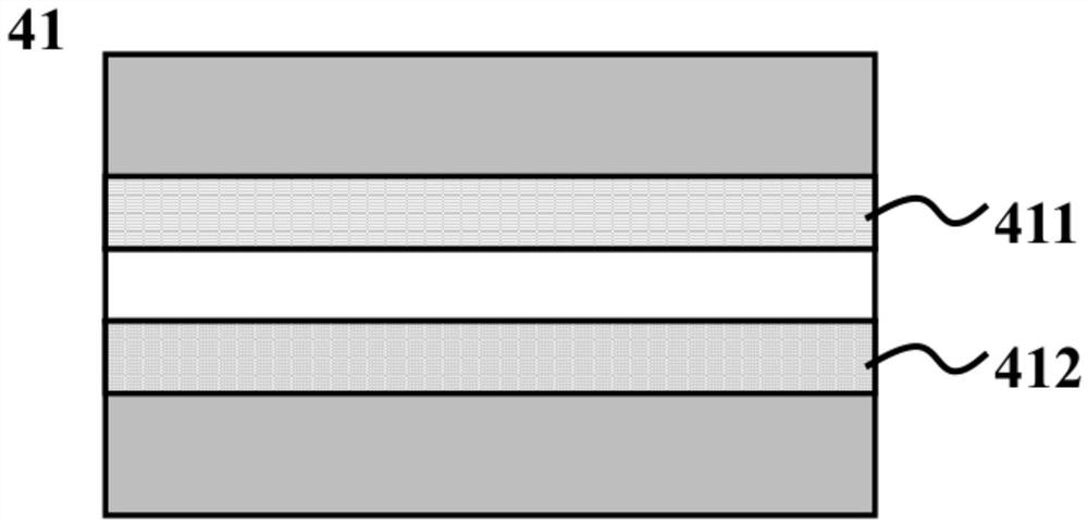
[0072] A method for regulating the electric field built in the active region of a deep ultraviolet light emitting diode. The other steps in this embodiment are the same as those in Embodiment 1. The difference is that the doping concentrations of the 411 and 412 quantum barrier doping layers in this embodiment are changed to 2e17.


PUM

PropertyMeasurementUnit
thicknessaaaaaaaaaa
thicknessaaaaaaaaaa

Abstract

The invention relates to a method for regulating and controlling an electric field built in an active region of a deep ultraviolet light-emitting diode, which belongs to the technical field of semiconductor photodiodes and sequentially comprises a substrate, a buffer layer, an n-type semiconductor electron injection layer, a multi-quantum well active layer, a p-type electron barrier layer, a p-type semiconductor hole injection layer, a p-type contact layer, a p-type electrode and an n-type electrode from bottom to top. The multi-quantum-well active layer comprises a plurality of units growing periodically, each unit comprises a quantum well and quantum barriers on the upper side and the lower side of the quantum well, Mg doping is carried out on the side, close to the quantum well, of the quantum barrier on the upper side of the quantum well, Si doping is carried out on the side, close to the quantum well, of the quantum barrier on the lower side of the quantum well, each quantum barrier is not fully doped, and Si doping is carried out on the side. The built-in electric field of the DUV LED is regulated and controlled through a selective doping method, the problems of wavelength red shift and efficiency attenuation caused by the overlarge built-in electric field are solved, meanwhile, electron and hole injection of the DUV LED is regulated and controlled, and the photoelectric property of the DUV LED is improved by inhibiting electron leakage and enhancing hole injection.

Description

technical field [0001] The invention relates to a method for regulating and controlling an electric field built in an active region of a deep ultraviolet light emitting diode, and belongs to the technical field of semiconductor photodiodes. Background technique [0002] AlGaN material is a wide-bandgap direct bandgap semiconductor with adjustable band gap in the range of 3.4eV~6.2eV. The corresponding emission wavelength range can be changed from 365nm to 200nm. It is the most suitable material for the preparation of deep ultraviolet light-emitting diodes. . Compared with traditional UV pump lamps, AlGaN-based deep-ultraviolet light-emitting diodes (DUV LEDs) have the advantages of less environmental hazard, low operating voltage, low energy consumption, and long service life. And DUV LED has great application value and broad market space in high-density optical storage, sterilization, air and water purification, biochemical experiments, anti-counterfeiting detection, displ...

Claims


Application Information

Patent Timeline
Patent Type & Authority Applications(China)
IPC IPC(8): H01L33/32H01L33/02H01L33/06H01L33/12H01L33/00
CPCH01L33/06H01L33/025H01L33/12H01L33/325H01L33/0075Y02P70/50
Inventor 刘超季泳辰
Owner SHANDONG UNIV
Why Eureka
Try Eureka