GaN-based LED epitaxial structure capable of improving carrier injection efficiency, and growth method thereof
An epitaxial structure and growth method technology, applied in the field of LED design and application, can solve problems such as electron leakage efficiency, energy band distortion of the light-emitting layer, and limiting the luminous efficiency of GaN-based LEDs, so as to improve chip quality, reduce lattice defects and larger The effect of stress
- Summary
- Abstract
- Description
- Claims
- Application Information
AI Technical Summary
Problems solved by technology
Method used
Image
Examples
Embodiment 1
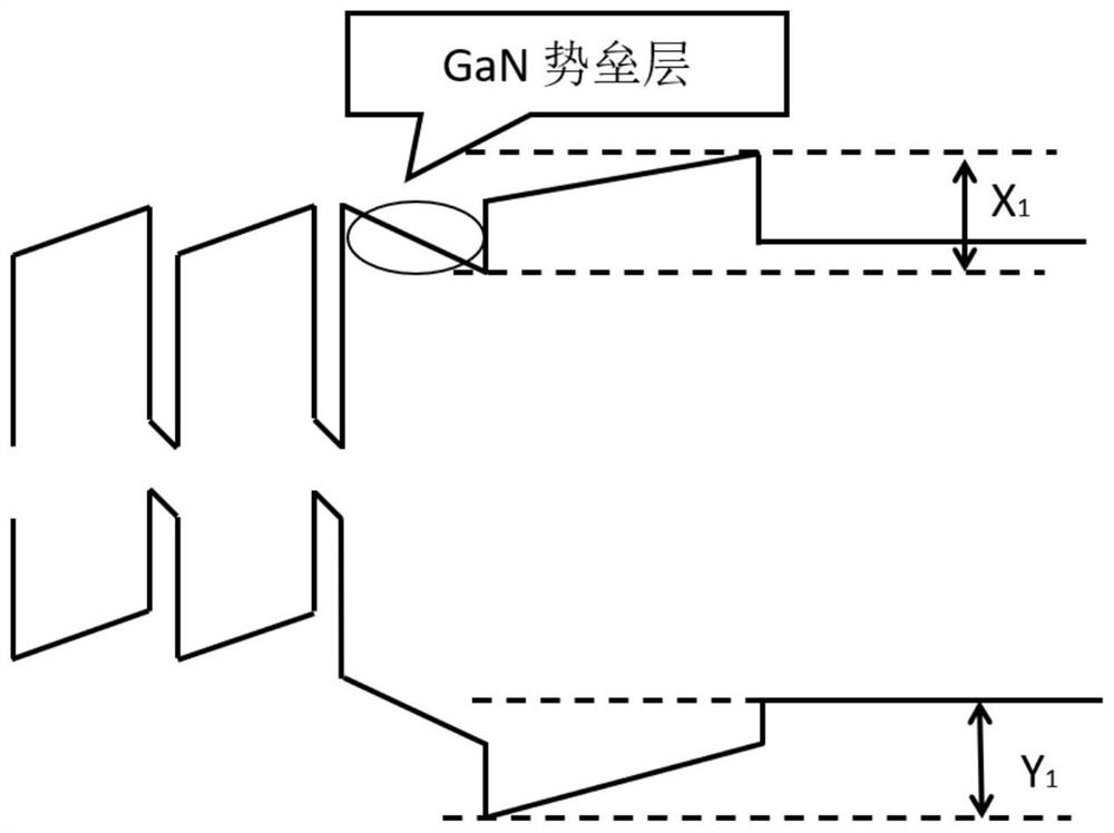
[0039] For the light-emitting layer in the epitaxial structure of this embodiment, see Figure 5 , growth method see Figure 4 . The specific growth method is as follows:
[0040] Step 101, processing the substrate:
[0041] In a hydrogen atmosphere, the sapphire substrate was annealed at a temperature of 1100 °C to clean the surface of the substrate.
[0042] Step 102, growing a low-temperature nucleation layer GaN:
[0043] At 550°C, the reaction chamber pressure is 500 Torr, ammonia gas and TMGa are fed in, and a low-temperature nucleation layer GaN with a thickness of 30nm is grown on the sapphire substrate.
[0044] Step 103, growing a non-doped n-GaN layer:
[0045] At 1100°C, keep the pressure of the reaction chamber at 500Torr, inject ammonia gas and TMGa, and continuously grow a non-doped u-GaN layer with a thickness of 2μm.
[0046] Step 104, growing a Si-doped n-GaN layer:
[0047] At 1100°C, keep the reaction chamber pressure at 500 Torr, and feed ammonia, T...
Embodiment 2
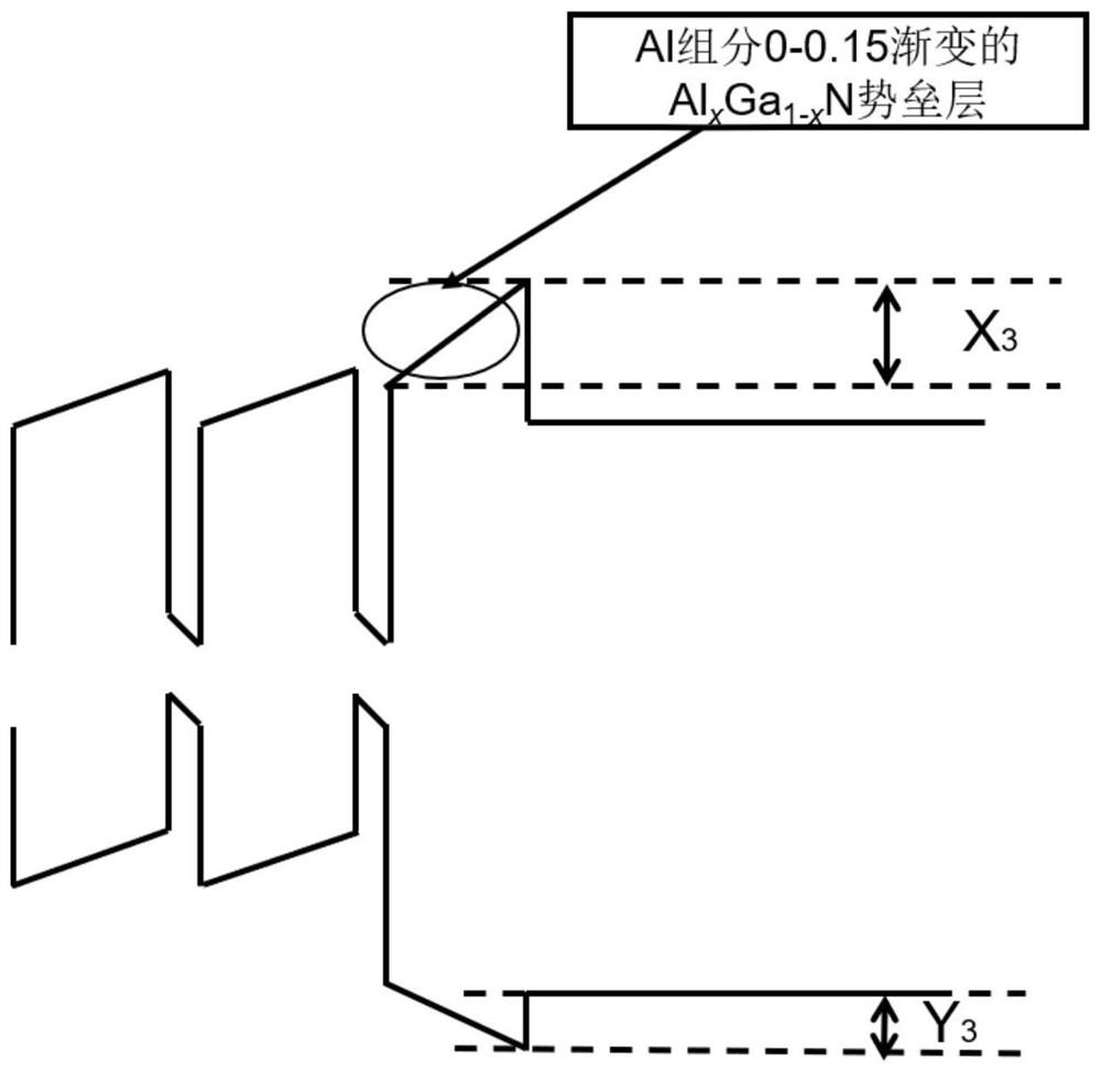
[0060] The specific growth method is as follows:
[0061] Step 201, processing the substrate:
[0062] In a hydrogen atmosphere, the sapphire substrate was annealed at a temperature of 1100 °C to clean the surface of the substrate.
[0063] Step 202, growing a low-temperature nucleation layer GaN:
[0064] At 550°C, the reaction chamber pressure is 500 Torr, ammonia gas and TMGa are fed in, and a low-temperature nucleation layer GaN with a thickness of 30nm is grown on the sapphire substrate.
[0065] Step 203, growing a non-doped n-GaN layer:
[0066] At 1100°C, keep the pressure of the reaction chamber at 500Torr, inject ammonia gas and TMGa, and continuously grow a non-doped u-GaN layer with a thickness of 2μm.
[0067] Step 204, growing a Si-doped n-GaN layer:
[0068] At 1100°C, keep the reaction chamber pressure at 500 Torr, and feed ammonia, TMGa and SiH 4 , continue to grow a layer of n-GaN layer doped with Si with a thickness of 3 μm and a stable doping concentra...
Embodiment 3
[0082] This embodiment adopts the traditional GaN-based LED epitaxial growth method, as follows:
[0083] Step 301, processing the substrate:
[0084] In a hydrogen atmosphere, the sapphire substrate was annealed at a temperature of 1100 °C to clean the surface of the substrate.
[0085] Step 302, growing a low-temperature nucleation layer GaN:
[0086] At 550°C, the reaction chamber pressure is 500 Torr, ammonia gas and TMGa are fed in, and a low-temperature nucleation layer GaN with a thickness of 30nm is grown on the sapphire substrate.
[0087] Step 303, growing a non-doped n-GaN layer:
[0088] At 1100°C, keep the pressure of the reaction chamber at 500Torr, inject ammonia gas and TMGa, and continuously grow a non-doped u-GaN layer with a thickness of 2μm.
[0089] Step 304, growing a Si-doped n-GaN layer:
[0090] At 1100°C, keep the reaction chamber pressure at 500 Torr, and feed ammonia, TMGa and SiH 4 , continue to grow a layer of n-GaN layer doped with Si with a...
PUM
| Property | Measurement | Unit |
|---|---|---|
| Thickness | aaaaa | aaaaa |
| Thickness | aaaaa | aaaaa |
Abstract
Description
Claims
Application Information
 - R&D
- Intellectual Property
- Life Sciences
- Materials
- Tech Scout
- Unparalleled Data Quality
- Higher Quality Content
- 60% Fewer Hallucinations
Browse by: Latest US Patents, China's latest patents, Technical Efficacy Thesaurus, Application Domain, Technology Topic, Popular Technical Reports.
© 2025 PatSnap. All rights reserved.Legal|Privacy policy|Modern Slavery Act Transparency Statement|Sitemap|About US| Contact US: help@patsnap.com


