Method for enhancing LED luminous efficiency based on 3D printing ferromagnetic layer
A 3D printing, luminous efficiency technology, applied in electrical components, circuits, semiconductor devices, etc., can solve the problems of high regularity requirements, high cost, high equipment and process requirements, etc., to improve radiation recombination rate and enhance luminous efficiency. , the effect of improving production efficiency
- Summary
- Abstract
- Description
- Claims
- Application Information
AI Technical Summary
Problems solved by technology
Method used
Image

Examples
Embodiment 1
[0031] A method based on 3D printing ferromagnetic layer to enhance LED luminous efficiency,
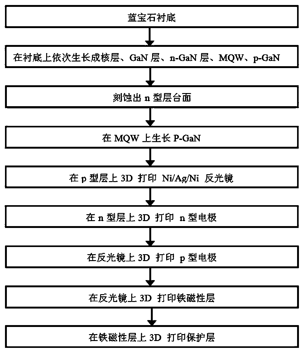
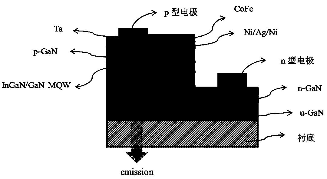
[0032] Step 1: Provide a sapphire substrate, and grow a low-temperature GaN nucleation layer, unintentionally doped GaN layer, n-GaN, InGaN / GaN MQW, and p-GaN epitaxial wafers sequentially on the substrate;
[0033] Step 2: Etching the n-type layer mesa on the epitaxial wafer, and the etching depth reaches the n-GaN layer;
[0034] Step 3: Write the motion path program of each 3D printing head according to the structural design, put the cleaned epitaxial wafer into the 3D printer as the substrate, and use a single or array 3D mirror material printing head to print thickness on the p-GaN layer 100nm ohmic contact mirror;
[0035] Print an n-type electrode with a thickness of 220nm on the n-type layer mesa using a single or array 3D n-type electrode material printing head;
[0036] Use a single or array 3D p-type electrode material printing head to print a p-type electrode with a thi...
Embodiment 2
[0041] A method based on 3D printing ferromagnetic layer to enhance LED luminous efficiency,
[0042] Step 1: Provide a sapphire substrate, and grow a low-temperature GaN nucleation layer, unintentionally doped GaN layer, n-GaN, InGaN / GaN MQW, and p-GaN epitaxial wafers sequentially on the substrate;
[0043] Step 2: Etching the n-type layer mesa on the epitaxial wafer, and the etching depth reaches the n-GaN layer;
[0044] Step 3: Write the motion path program of each 3D printing head according to the structural design, put the cleaned epitaxial wafer into the 3D printer as the substrate, and use a single or array 3D mirror material printing head to print thickness on the p-GaN layer 150nm ohmic contact mirror;
[0045] Use a single or array type 3D n-type electrode material printing head to print n-type electrodes with a thickness of 300nm on the n-type layer mesa;
[0046] Use a single or array 3D p-type electrode material printing head to print a p-type electrode with a...
Embodiment 3
[0051] A method based on 3D printing ferromagnetic layer to enhance LED luminous efficiency,
[0052] Step 1: Provide a sapphire substrate, and grow a low-temperature GaN nucleation layer, unintentionally doped GaN layer, n-GaN, InGaN / GaN MQW, and p-GaN epitaxial wafers sequentially on the substrate;
[0053] Step 2: Etching the n-type layer mesa on the epitaxial wafer, and the etching depth reaches the n-GaN layer;
[0054] Step 3: Write the motion path program of each 3D printing head according to the structural design, put the cleaned epitaxial wafer into the 3D printer as the substrate, and use a single or array 3D mirror material printing head to print thickness on the p-GaN layer 200nm ohmic contact mirror;
[0055] Use a single or array type 3D n-type electrode material printing head to print n-type electrodes with a thickness of 150nm on the n-type layer mesa;
[0056] Use a single or array 3D p-type electrode material printing head to print a p-type electrode with a...
PUM
| Property | Measurement | Unit |
|---|---|---|
| thickness | aaaaa | aaaaa |
| thickness | aaaaa | aaaaa |
| thickness | aaaaa | aaaaa |
Abstract
Description
Claims
Application Information
 - R&D
- Intellectual Property
- Life Sciences
- Materials
- Tech Scout
- Unparalleled Data Quality
- Higher Quality Content
- 60% Fewer Hallucinations
Browse by: Latest US Patents, China's latest patents, Technical Efficacy Thesaurus, Application Domain, Technology Topic, Popular Technical Reports.
© 2025 PatSnap. All rights reserved.Legal|Privacy policy|Modern Slavery Act Transparency Statement|Sitemap|About US| Contact US: help@patsnap.com