Epitaxial structures and growth methods of gan-based LEDs

An epitaxial structure and epitaxial growth technology, used in semiconductor devices, electrical components, circuits, etc., can solve the problems of light-emitting layer distortion, epitaxial crystal quality deterioration, low activation rate, etc., to improve the radiation recombination rate and the overall performance of the device. , reduce the effect of non-radiative recombination

Active Publication Date: 2019-07-12
YANGZHOU UNIV
View PDF5 Cites 0 Cited by
  • Summary
  • Abstract
  • Description
  • Claims
  • Application Information

AI Technical Summary

Problems solved by technology

However, the AlGaN electron blocking layer will also form a hole barrier on the valence band, reducing the hole injection efficiency; and due to the polarization effect between the last GaN barrier layer and the AlGaN electron blocking layer, it is not conducive to improving the hole injection efficiency. Injection and Electron Leakage Issues
In addition, because the P-type Mg-doped ionization activation rate of the AlGaN electron blocking layer is very low, this leads to a low hole concentration in AlGaN, and as the composition of Al increases, the quality of the epitaxial crystal deteriorates, and serious lattice defects and Relatively large stress, which causes a large distortion of the energy band of the light-emitting layer, affects the recombination rate of electrons and holes
Moreover, as the injection current further increases, the valence band energy band difference at the AlGaN / GaN interface will widen, which will also make it more difficult for holes to be effectively injected into the light-emitting layer.

Method used


Image

  • Epitaxial structures and growth methods of gan-based LEDs
  • Epitaxial structures and growth methods of gan-based LEDs
  • Epitaxial structures and growth methods of gan-based LEDs

Examples


Embodiment 1

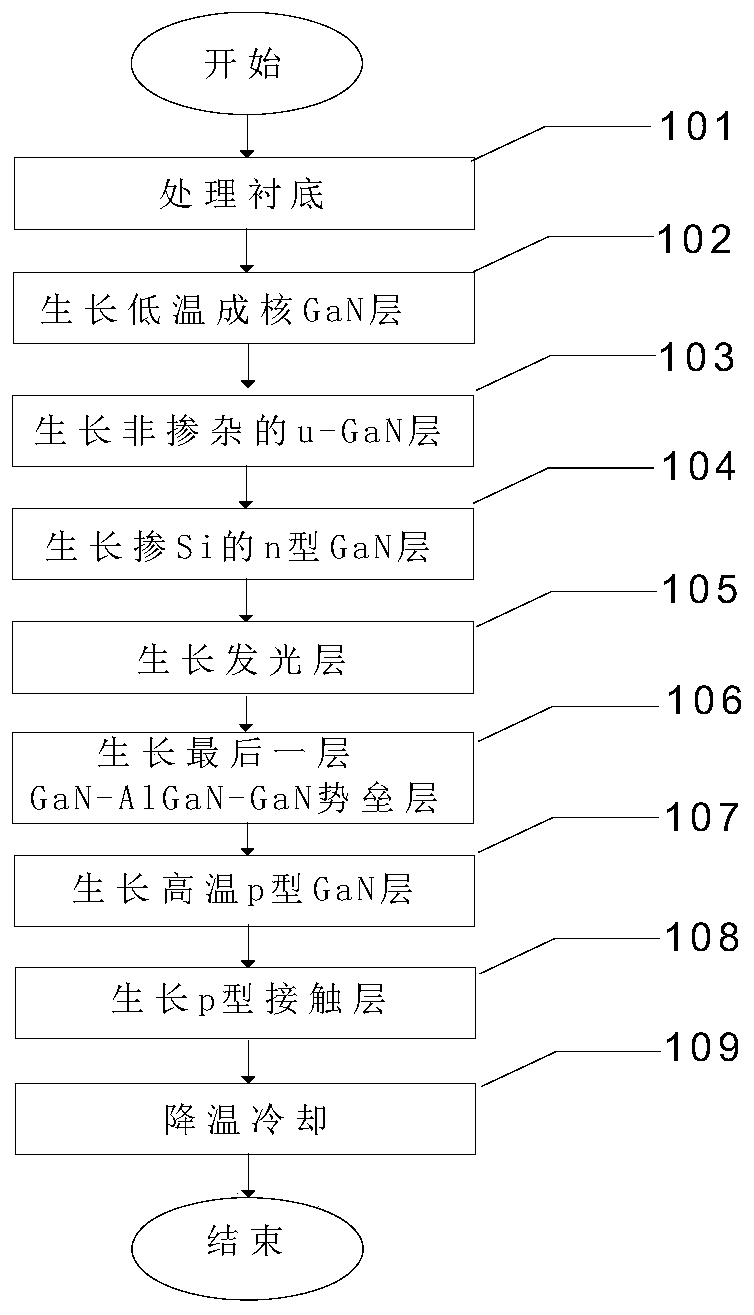
[0042] The application examples of the LED epitaxial growth method of the present invention are provided below, using VEECO MOCVD to grow high-brightness GaN-based LED epitaxial wafers. Using high-purity H 2 or high purity N 2 or high purity H 2 with high purity N 2 mixed gas as carrier gas, high-purity NH 3 (NH 3 Purity is 99.999%) as N source, metal-organic source trimethylgallium (TMGa) and metal-organic source triethylgallium (TEGa), trimethylindium (TMIn) as indium source, N-type dopant is silane ( SiH 4 ), trimethylaluminum (TMAl) as the aluminum source, and the P-type dopant as magnesium dicene (CP 2 Mg), the substrate is (0001) sapphire, and the reaction pressure is between 100Torr and 1000Torr.

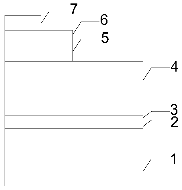
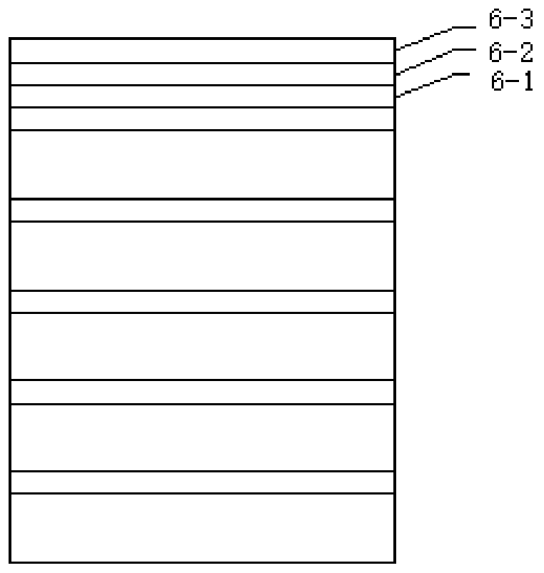
[0043] see figure 2 and image 3 , the invention discloses a LED epitaxial layer growth method for improving luminous efficiency, and an LED epitaxial structure prepared according to the epitaxial method, the epitaxial structure sequentially includes: a substrate 1,...


PUM


Abstract

The invention discloses a GaN LED epitaxial structure and a growth method thereof, which sequentially include processing a substrate, growing a low-temperature nucleation layer, growing a non-doped low-temperature u-GaN layer, growing a Si-doped n-GaN layer, and growing a light-emitting layer , growing a GaN-AlGaN-GaN barrier layer, growing a P-type GaN layer, and cooling down. The present invention adopts the GaN-AlGaN-GaN combined structure, which can effectively provide electron potential barriers to limit the leakage of electrons to the P-type region, reduce the non-radiative recombination of electrons and holes in the P-type region, and effectively improve the efficiency of the holes. The implantation from the P electrode to the active area improves the optoelectronic performance of the device; the removal of the traditional AlGaN electron blocking layer avoids serious lattice defects at the material interface when growing a thicker and highly Mg-doped p-type AlGaN layer And the problem of large stress, it also avoids the influence of long-term high-temperature growth on the MQW layer, and improves the chip quality.

Description

technical field [0001] The invention relates to the field of LED design and application, in particular to an LED epitaxy structure with improved hole injection layer and light emitting layer structure and a growth method thereof. Background technique [0002] GaN light-emitting diodes (LEDs) will completely replace traditional incandescent and fluorescent lamps in backlighting, energy-saving lighting and general lighting due to their advantages of high brightness, low power consumption, long life, and low power. However, the photoelectricity of III-nitride devices Performance is significantly impaired by efficiency degradation, which is due to the rapid decrease in luminous efficacy in GaN-based LEDs due to the increase in injected current. Therefore, the industry has been working on improving the LED efficiency drop to improve the performance of GaN LEDs. At present, researchers have proposed that the main reasons for the efficiency drop are poor carrier injection inside t...

Claims


Application Information

Patent Timeline
Patent Type & Authority Patents(China)
IPC IPC(8): H01L33/00H01L33/14H01L33/32
CPCH01L33/0075H01L33/145H01L33/32H01L33/325
Inventor 程立文曹常锐曾祥华马剑徐作政
Owner YANGZHOU UNIV
Why Eureka
Try Eureka