Hexagonal boron nitride deep ultraviolet photoelectric detector with embedded MSM structure and preparation method thereof
A technology of hexagonal boron nitride and deep ultraviolet light, which is applied in the field of hexagonal boron nitride deep ultraviolet photodetectors and its preparation, can solve the problems of unsatisfactory practical application, low responsivity and detection sensitivity of hexagonal boron nitride detectors , to prevent shedding and contamination, ensure stability, improve responsiveness and response speed
- Summary
- Abstract
- Description
- Claims
- Application Information
AI Technical Summary
Problems solved by technology
Method used
Image
Examples
Embodiment 1
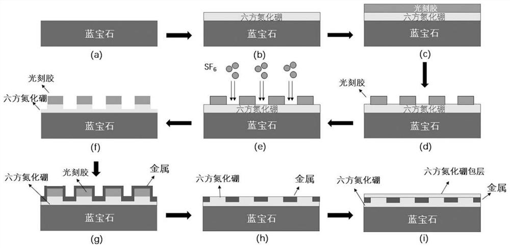
[0025] (1) successively the c-plane sapphire substrate 1 was cleaned by ultrasonic waves for 10 min each by acetone, ethanol and deionized water, and finally the c-plane sapphire substrate 1 was blown dry with a nitrogen gun for subsequent use;
[0026] (2) Put the c-plane sapphire substrate 1 into the chamber of the low pressure chemical vapor deposition equipment, pass nitrogen, boron trichloride and ammonia gas, the flow ratio is 200sccm:10sccm:30sccm, and grow at 1350°C for 20min , a hexagonal boron nitride layer 2 with a thickness of 400 nm is obtained on the surface of the c-plane sapphire substrate 1;
[0027] (3) In-situ annealing at 1650°C for 10min;
[0028] (4) Uniformly coat a layer of photoresist on the surface of the sample treated in step (3), and then perform photolithography treatment: the photoresist model is BP 212-37S, and the photolithography process includes uniform glue: low rotation speed 500rpm, High speed 4500rpm; pre-bake: remove solvent after 90℃ h...
Embodiment 2
[0034] (1) successively cleaning the c-plane sapphire substrate 1 by ultrasonic cleaning of acetone, ethanol and deionized water for 10min, and drying the c-plane sapphire substrate 1 with a nitrogen gun for subsequent use;
[0035] (2) Put the c-axis sapphire substrate 1 into the magnetron sputtering apparatus, and evacuate to a background vacuum of 5×10 -3Pa, at a temperature of 600°C, argon and nitrogen gas were introduced, and the flow ratio was 50sccm:50sccm, and the hexagonal boron nitride target was sputtered, and the sputtering time was 40 min to form a 400 nm thick hexagonal boron nitride layer 2.
[0036] (3) Uniformly coat a layer of photoresist on the surface of the device treated in step (3) and then carry out photolithography processing: the photoresist model is BP 212-37S of Beijing Kehua Company, and the photolithography process includes uniform glue: Low speed 500rpm, high speed 4500rpm; Pre-baking: 90°C hot plate baking for 20min to remove solvent; Exposure: ...
PUM
| Property | Measurement | Unit |
|---|---|---|
| width | aaaaa | aaaaa |
| thickness | aaaaa | aaaaa |
| thickness | aaaaa | aaaaa |
Abstract
Description
Claims
Application Information
 - Generate Ideas
- Intellectual Property
- Life Sciences
- Materials
- Tech Scout
- Unparalleled Data Quality
- Higher Quality Content
- 60% Fewer Hallucinations
Browse by: Latest US Patents, China's latest patents, Technical Efficacy Thesaurus, Application Domain, Technology Topic, Popular Technical Reports.
© 2025 PatSnap. All rights reserved.Legal|Privacy policy|Modern Slavery Act Transparency Statement|Sitemap|About US| Contact US: help@patsnap.com


