
Tunneling photodiode suitable for high-energy photon detection and preparation method thereof

A photodiode, high-energy photon technology, applied in photovoltaic power generation, circuits, electrical components, etc., to achieve the effects of high absorption and conversion efficiency, improved detection efficiency, and improved signal-to-noise ratio

Pending Publication Date: 2022-05-27
SOUTHEAST UNIV
View PDF0 Cites 0 Cited by
  • Summary
  • Abstract
  • Description
  • Claims
  • Application Information

AI Technical Summary

Problems solved by technology

Since quantum dots can only absorb photons with lower energy, the above-mentioned quantum dot / perovskite field emission tunneling diode can only be used for near-infrared and visible light detection.

Method used


Image

  • Tunneling photodiode suitable for high-energy photon detection and preparation method thereof
  • Tunneling photodiode suitable for high-energy photon detection and preparation method thereof
  • Tunneling photodiode suitable for high-energy photon detection and preparation method thereof

Examples


Embodiment Construction

[0052] The present invention will be further explained below in conjunction with the accompanying drawings.

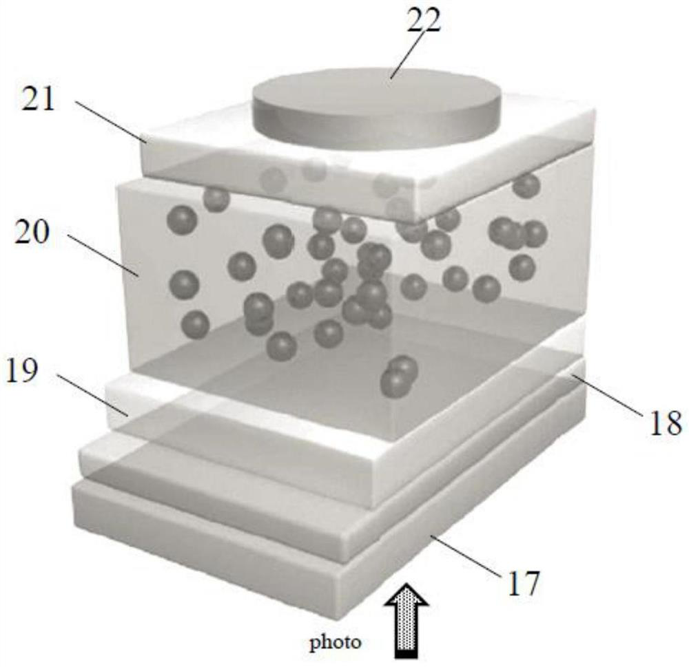
[0053] like Figure 5 As shown, a tunneling photodiode suitable for high-energy photon detection includes a perovskite intrinsic absorption layer 24, and a perovskite P-type layer 25 and a perovskite perovskite P-type layer 25 and a perovskite are respectively disposed at both ends of the perovskite intrinsic absorption layer 24. The mineral N-type layer 23 forms a perovskite PIN junction. Narrow band gap semiconductor quantum dots 26 are respectively arranged near the P / I junction region and the N / I junction region of the perovskite PIN junction to form quantum dot energy level traps.

[0054] like Image 6 As shown, the perovskite intrinsic absorption layer 24 uses a perovskite single crystal as the absorber of high-energy photons. When used for X-ray detection, the thickness of the perovskite intrinsic absorption layer is 1-10 mm. The thickness of the perovskite ...


PUM

PropertyMeasurementUnit
thicknessaaaaaaaaaa
thicknessaaaaaaaaaa

Abstract

The invention discloses a tunneling photodiode suitable for high-energy photon detection and a preparation method of the tunneling photodiode, and the tunneling photodiode adopts an intrinsic perovskite crystal with very high thickness as a high-energy photon absorber to obtain relatively high photon absorption and conversion efficiency. A perovskite P-type layer and a perovskite N-type layer respectively grow at two ends of an intrinsic perovskite crystal by using a solution doping epitaxy method to form a perovskite PIN junction, and a junction region depletion layer potential barrier is used for inhibiting dark current and noise. And narrow-band-gap quantum dots are epitaxially grown in the junction region to form an energy band trap. When high-energy photons are incident, photon-generated carriers generated by the perovskite intrinsic absorber are injected into the quantum dot energy level trap, tunneling field emission occurs, and high-gain light current is obtained. Compared with a conventional high-energy photon PIN detection structure, due to the introduction of the tunneling field emission structure, high photocurrent gain can be obtained. Compared with a high-energy photon avalanche diode detection structure, since no random avalanche effect is generated, shot noise is relatively low.

Description

technical field [0001] The invention relates to the field of high-energy photon detection and imaging, in particular to a tunneling photodiode suitable for high-energy photon detection and a preparation method thereof. Background technique [0002] The detection of high-energy photons such as X-rays and γ-rays has important applications in the fields of nuclear medicine, aerospace, and industrial non-destructive testing. People have been working hard to develop high-performance high-energy photon detectors. Since high-energy photons such as X-rays and γ-rays have high energy and strong penetrating ability, the photocurrent obtained in the process of high-energy photon detection is often much smaller than that obtained by visible light detection. Reducing the detection noise of high-energy photons and increasing the photocurrent amplitude are the goals that people have been working on. [0003] In X-ray and γ-ray detection, people usually use PIN diode detection structure. ...

Claims


Application Information

Patent Timeline
Patent Type & Authority Applications(China)
IPC IPC(8): H01L51/42H01L51/48
CPCH10K71/10H10K30/40Y02E10/549
Inventor 雷威王昕宋波李青张晓兵朱卓娅赵志伟徐玉冰潘禹竹李雨巍
Owner SOUTHEAST UNIV
Learn More