Preparation method of gallium nitride epitaxial structure

An epitaxial structure, gallium nitride technology, applied in the field of preparation of gallium nitride epitaxial structure, can solve problems such as poor heat transfer capability, achieve the effects of reducing thermal resistance, shortening transmission distance, and reducing interface thermal resistance

Active Publication Date: 2022-04-01
中电化合物半导体有限公司
View PDF8 Cites 0 Cited by
  • Summary
  • Abstract
  • Description
  • Claims
  • Application Information

AI Technical Summary

Problems solved by technology

[0005] Aiming at the deficiencies and defects in the prior art, the present invention provides a method for preparing a gallium nitride epitaxial structure, in which diamond with high thermal conductivity is introduced into the epitaxial layer, Used to improve the problem of poor heat transfer capability of GaN-based HEMT devices

Method used


Image

  • Preparation method of gallium nitride epitaxial structure
  • Preparation method of gallium nitride epitaxial structure
  • Preparation method of gallium nitride epitaxial structure

Examples


preparation example Construction

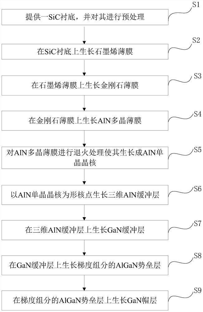
[0056] The present invention provides a method for preparing a gallium nitride epitaxial structure, which uses TMAL, TMGA and NH. 3 As the source, gallium (Ga) source and nitrogen (N) source, H 2 Or N 2 As the carrier gas.

[0057] See Figures 1 to 10 The preparation method of the gallium nitride epitaxial structure of the present invention includes at least the following steps:

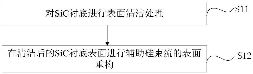
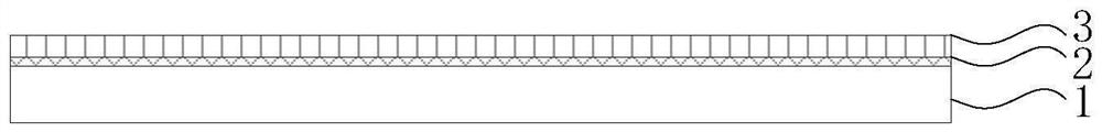
[0058] S1, a SiC substrate 1 is provided, and the SiC substrate 1 is pretreated;

[0059] S2, grown graphene film 2 on the SiC substrate 1 after the pretreatment;

[0060] S3, grown diamond film 3 on the graphene film 2;

[0061] S4 growth AlN polycrystalline film 4 on diamond film 3;

[0062] S5, annealing the ALN polycrystalline film 4 to grow into AlN single crystal nucleus 5;

[0063] S6, the three-dimensional AlN buffer layer 6 is grown by AlN single crystal nucleation 5;

[0064] S7 grows GaN buffer layer 7 on three-dimensional AlN buffer layer 6;

[0065] S8, the Alga barrier layer 8 of the gradie...


PUM

PropertyMeasurementUnit
thicknessaaaaaaaaaa
thicknessaaaaaaaaaa
thicknessaaaaaaaaaa

Abstract

The invention provides a preparation method of a gallium nitride epitaxial structure, and the preparation method comprises the steps: providing a silicon carbide substrate, and carrying out the pretreatment of the silicon carbide substrate; a graphene thin film, a diamond thin film, a three-dimensional aluminum nitride buffer layer, a gallium nitride buffer layer, an AlGaN barrier layer with gradient components and a gallium nitride cap layer are sequentially grown on the silicon carbide substrate after pretreatment, and the three-dimensional aluminum nitride buffer layer is a grown aluminum nitride polycrystalline thin film firstly; and annealing the aluminum nitride polycrystalline thin film to enable the aluminum nitride polycrystalline thin film to grow into an aluminum nitride single-crystal crystal nucleus, and continuing to grow a three-dimensional aluminum nitride buffer layer on the basis of the aluminum nitride single-crystal crystal nucleus. According to the method, the graphene and the diamond are used as the rapid heat conduction layer, the thin gallium nitride buffer layer greatly shortens the heat transmission distance of the radio frequency device, the working thermal resistance of the device can be effectively reduced, and the working efficiency of the HEMT device is improved.

Description

Technical field [0001] The present invention relates to the field of semiconductor epitaxial growth, and more particularly to a method of preparing a gallium nitride epitaxial structure. Background technique [0002] Gallium nitride (GaN) material due to its wide disable band width (3.4 eV), high thermal conductivity, high electron saturation drift speed, high-shifting electric field corrosion resistance and anti-radiation, etc., good thermodynamics, In the fields of high frequency, high temperature, high pressure, high-power RF devices and other areas. [0003] AlgaN / GaN heterojunction has a very strong piezoelectric polarization and spontaneous polarization effect, which can form high mobility and high concentration of two-dimensional electron gas (2deg) in the heterogeneous interface, which can prepare A1GAN / GaN. High electron mobility transistors (HIGH Electron Mobility Transistor). A1GAN / GaN Hemt is widely used in radar, 5G base station, etc. [0004] At present, the s...

Claims


Application Information

Patent Timeline
Patent Type & Authority Applications(China)
IPC IPC(8): C30B29/40C30B25/16C30B25/18C30B28/14C23C16/02C23C16/27C30B33/02H01L21/02
Inventor 唐军冯欢欢潘尧波
Owner 中电化合物半导体有限公司
Why Eureka
Try Eureka