Preparation process of hyperspectral photoelectric detector
A technology of photodetector and preparation process, applied in spectrometry/spectrophotometry/monochromator, electric solid device, optical radiation measurement, etc., can solve the problems of low integration and complex system, etc.
- Summary
- Abstract
- Description
- Claims
- Application Information
AI Technical Summary
Problems solved by technology
Method used
Image
Examples
preparation example Construction
[0026] A preparation process of a hyperspectral photodetector, comprising the following steps:
[0027] S1. Firstly, the quartz glass substrate is cleaned, and then its surface is treated;
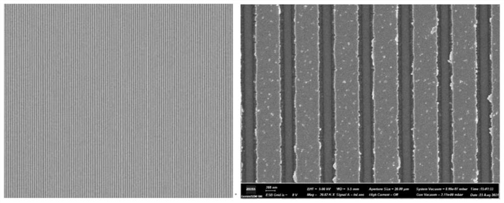
[0028] S2. Using electron beam lithography to make a pattern of the grating array on the quartz glass substrate, and then depositing metal and cleaning to obtain the metal grating array of the first layer;
[0029] S3. Deposit a layer of SU8 dielectric material with a thickness of 1.5 μm on the metal grating array by using the spin coating method, and fix the SU8 dielectric layer on the metal grating array of the first layer by ultraviolet exposure and heating, and finally obtain a narrowband beam splitter array ;
[0030] S4. Selecting InP-based InGaAs as the material for preparing the detector array, preparing the detector array and the corresponding readout circuit for flip-chip bonding;
[0031] S5. Chip-integrate the narrowband beam splitter array and the detector array.
[0032] F...
Embodiment 1
[0039] A preparation process of a hyperspectral photodetector, comprising the following steps:
[0040] S1. Firstly, the quartz glass substrate is cleaned, and then its surface is treated;
[0041] S2, using electron beam lithography to make a pattern of the grating array on the quartz glass substrate, and then depositing metal and cleaning to obtain the metal grating array of the first layer;
[0042] S3. Deposit a layer of SU8 dielectric material with a thickness of 1.5 μm on the metal grating array by using the spin coating method, and fix the SU8 dielectric layer on the metal grating array of the first layer by ultraviolet exposure and heating, and finally obtain a narrowband beam splitter array ;
[0043] S4. Selecting InP-based InGaAs as the material for preparing the detector array, preparing the detector array and the corresponding readout circuit for flip-chip bonding;
[0044] S5. Chip-integrate the narrowband beam splitter array and the detector array.
Embodiment 2
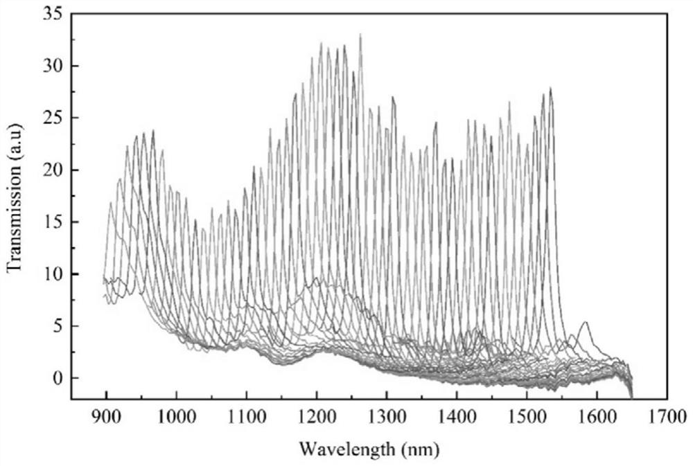
[0046] On the basis of Example 1, in the step S5, when the narrow-band beam splitter array and the detector array are patch-integrated, the beam splitter array is arranged in the form of a line array and sequentially arranged into 900-1500nm beam splitter modules, The beam splitter module of each channel corresponds to a detector pixel.
PUM
 Abstract
Description
Claims
Application Information
 - Generate Ideas
- Intellectual Property
- Life Sciences
- Materials
- Tech Scout
- Unparalleled Data Quality
- Higher Quality Content
- 60% Fewer Hallucinations
Browse by: Latest US Patents, China's latest patents, Technical Efficacy Thesaurus, Application Domain, Technology Topic, Popular Technical Reports.
© 2025 PatSnap. All rights reserved.Legal|Privacy policy|Modern Slavery Act Transparency Statement|Sitemap|About US| Contact US: help@patsnap.com


