
Method for etching pattern by hard mask and preparation method of refrigeration infrared detector

A technology of hard mask and hard mask layer, which is applied in semiconductor devices, final product manufacturing, sustainable manufacturing/processing, etc. It can solve the problems of reducing the yield and performance of cooled infrared detectors, undercutting, and affecting the normal progress of the process, etc. , to achieve the effect of reducing undercutting, improving yield, and reducing filling defects

Pending Publication Date: 2022-03-11
ZHEJIANG JUEXIN MICROELECTRONICS CO LTD
View PDF0 Cites 0 Cited by
  • Summary
  • Abstract
  • Description
  • Claims
  • Application Information

AI Technical Summary

Problems solved by technology

[0004] However, in SiO 2 During the etching process of the hard mask, the phenomenon of undercut (undercut) is easy to occur, which affects the normal progress of the subsequent process and reduces the yield and performance of the cooled infrared detector.

Method used


Image

  • Method for etching pattern by hard mask and preparation method of refrigeration infrared detector
  • Method for etching pattern by hard mask and preparation method of refrigeration infrared detector
  • Method for etching pattern by hard mask and preparation method of refrigeration infrared detector

Examples


preparation example Construction

[0033] The preparation method of the current cooling infrared detector comprises the following steps:

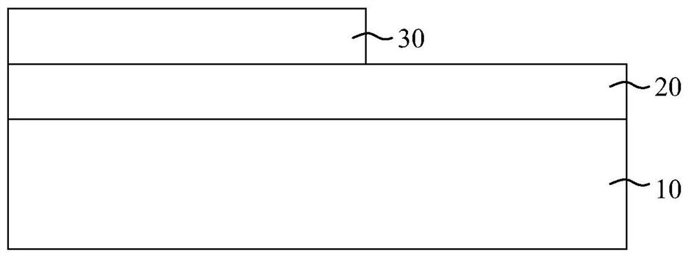
[0034] like Figure 1a As shown, step S11: a superlattice substrate 10 is provided, and SiO is formed on the superlattice substrate 10 2 hard mask layer 20 .

[0035] like Figure 1b As shown, step S12: forming a patterned photoresist layer 30 on the hard mask layer 20, the patterned photoresist layer 30 has a pattern, and the pattern is used to form a mesa.

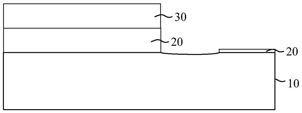
[0036] like Figure 1c As shown, step S13: using the patterned photoresist layer 30 as a mask to etch the SiO at one time 2 hard mask layer 20 to transfer the pattern to the SiO 2 hard mask layer 20 and expose the superlattice substrate 10 . At this time, due to pattern effect, in the SiO 2 There will be SiO in the etched area of ​​the hard mask layer 20 2 Material remains, resulting in undercutting. In addition, the SiO after etching 2 The hard mask layer 20 is prone to breakage.

[0037] According to the a...


PUM

PropertyMeasurementUnit
thicknessaaaaaaaaaa

Abstract

According to the method for etching the pattern by the hard mask and the preparation method of the refrigeration infrared detector provided by the invention, the method for etching the pattern by the hard mask completes the etching of the pattern by the hard mask through a one-time photoetching process and a two-time or three-time etching process, and forms a double-step etching pattern at the same time, thereby reducing the generation of an undercutting phenomenon, and improving the yield of the refrigeration infrared detector. Therefore, the internal stress of the etched side wall is relieved, the conductivity of the step area is improved, the filling defects generated when substances are filled on the step subsequently are reduced, and the yield of the device in the subsequent process and the performance of the device are improved. And the patterned photoresist layer is used as a mask to etch the hard mask layer at the second opening, so that a step-shaped hard mask layer can be formed, and the phenomenon of breakage of the hard mask layer is reduced.

Description

technical field [0001] The invention relates to the technical field of cooling infrared detectors, in particular to a method for etching patterns on a hard mask. Background technique [0002] In the current 1-3 generation semiconductor manufacturing, ICP etching (Inductively Coupled Plasma, inductively coupled plasma etching) or RIE etching (Reactive Ion Etching, reactive ion etching) is an essential process step. In ICP etching or RIE etching, SiO is usually used 2 As a hard coat layer to get good SiO 2 profile. [0003] In recent years, ICP etching or RIE etching, as a common plasma dry etching, can achieve good etching effects when etching materials such as silicon, silicon dioxide, and III-V compounds. Therefore, ICP Etching or RIE etching is widely used in the fabrication process of various optoelectronic devices. At present, people have used this technology to make SiO2 for cooling infrared detectors based on GaSb materials. 2 hard mask etch process. SiO 2 The e...

Claims


Application Information

Patent Timeline
Patent Type & Authority Applications(China)
IPC IPC(8): H01L21/308H01L21/3213H01L31/18
CPCH01L21/3081H01L21/3086H01L21/32139H01L31/184H01L31/1852Y02P70/50
Inventor 杨天伦李明霞
Owner ZHEJIANG JUEXIN MICROELECTRONICS CO LTD
Learn More