All-ferroelectric semiconductor PN junction thin film device and preparation method thereof
A thin-film device, PN junction technology, applied in semiconductor devices, electrical components, circuits, etc., can solve problems such as destructive reading of data, and achieve the effect of reliable theoretical value
- Summary
- Abstract
- Description
- Claims
- Application Information
AI Technical Summary
Problems solved by technology
Method used
Image

Examples
Embodiment 1
[0059] (1) BiFeO 3 Target and BiFe 0.9 Zn 0.1 o 3 Target preparation:
[0060] Will 99.9% Bi 2 o 3 and 99.9% Fe 2 o 3 Weigh the total mass of 15g powder according to the molar ratio of 1.3:1, pre-sinter at 630°C for 2 hours after fully mixing, grind to powder after cooling down to room temperature, then pre-sinter at 730°C for 2 hours, and grind to powder after cooling down to room temperature shape. Then, the ground powder was pressed into tablets and calcined at 830° C. for 40 min to obtain a BFO target. The surface of the calcined target was smoothed with sandpaper, rinsed with alcohol and dried for later use.
[0061] Will 99.9% Bi 2 o 3 , 99.9% Fe 2 o 3 And 99.9% ZnO with a molar ratio of 1.3:0.9:0.1. Weigh the total mass as 15g powder, mix well and pre-sinter at 630°C for 2h, then grind to powder after cooling down to room temperature, and then pre-sinter at 730°C for 2h again, After cooling down to room temperature, grind to powder. Then, the ground powde...
Embodiment 2
[0071] (1) BiFeO 3 Target and BiFe 0.9 Zn 0.1 o 3 Target material preparation: same as Example 1.
[0072] (2) Cleaning treatment of the substrate: the same as in Embodiment 1.
[0073] (3) Preparation of bottom electrode: Same as Example 1.
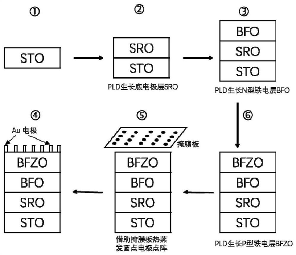
[0074] (4) Preparation of ferroelectric BFO / BFZO bilayer film:
[0075] Keep the temperature and oxygen pressure in step (3) constant, continue to use the pulsed laser deposition method to make the high-energy pulsed laser bombard the BFZO target and the BFO target in sequence, and deposit 100nm BFZO film and 100nm BFO film on the bottom electrode in turn to form a double layer ferroelectric film.
[0076] (5) Preparation of top electrode: Same as Example 1.
[0077] The performance of the ferroelectric diode of the all-ferroelectric semiconductor PN junction thin film device prepared in this example is opposite to that of Example 1.
Embodiment 3
[0079] (1) BiFeO 3 Target and BiFe 0.9 Zn 0.1 o 3 Target preparation:
[0080] Will 99.9% Bi 2 o 3 and 99.9% Fe 2 o 3 Weigh the total mass of 15g powder at a molar ratio of 1.3:1, pre-sinter at 600°C for 5 hours after mixing thoroughly, grind to powder after cooling down to room temperature, then pre-sinter at 750°C for 2 hours, and grind to powder after cooling down to room temperature shape. Then, the ground powder was pressed into tablets and calcined at 820° C. for 60 min to obtain a BFO target. The surface of the calcined target was smoothed with sandpaper, rinsed with alcohol and dried for later use.
[0081] Will 99.9% Bi 2 o 3 , 99.9% Fe 2 o 3 And 99.9% ZnO with a molar ratio of 1.3:0.9:0.1. Weigh the total mass as 15g powder, mix well and pre-sinter at 650°C for 3h, then grind to powder after cooling down to room temperature, and then pre-sinter at 700°C for 5h again, After cooling down to room temperature, grind to powder. Then, the ground powder was pre...
PUM
| Property | Measurement | Unit |
|---|---|---|
| Thickness | aaaaa | aaaaa |
| Diameter | aaaaa | aaaaa |
| Thickness | aaaaa | aaaaa |
Abstract
Description
Claims
Application Information
 - Generate Ideas
- Intellectual Property
- Life Sciences
- Materials
- Tech Scout
- Unparalleled Data Quality
- Higher Quality Content
- 60% Fewer Hallucinations
Browse by: Latest US Patents, China's latest patents, Technical Efficacy Thesaurus, Application Domain, Technology Topic, Popular Technical Reports.
© 2025 PatSnap. All rights reserved.Legal|Privacy policy|Modern Slavery Act Transparency Statement|Sitemap|About US| Contact US: help@patsnap.com