


Quick Research
Generate reliable direction feasibility study reports for your R&D in just a few steps.

Technical Q&A
Discover and master advanced knowledge NOW. Basics, ideas, possibilities, all at once.

Find Solutions
As an expert in R&D theories, this can generate solutions to your technical problems instantly.

Evaluate Feasibility
Analyze your overall solution with one click, know your potential R&D risks in advance.

Monitor Landscape
Get weekly tech updates, stay abreast of the latest tech innovations and key insights.
Light emitting diode and manufacturing method
A technology of light-emitting diodes and electrodes, which is applied to electrical components, circuits, semiconductor devices, etc., can solve the problems of easy adsorption of glue gas on the surface of the chip, poor adhesion and compactness, and damage to semiconductor epitaxial stacks, so as to improve the appearance yield , Improve reliability, improve the effect of photoelectric performance
- Summary
- Abstract
- Description
- Claims
- Application Information
AI Technical Summary
Problems solved by technology
Method used
Image

Examples
Embodiment 1
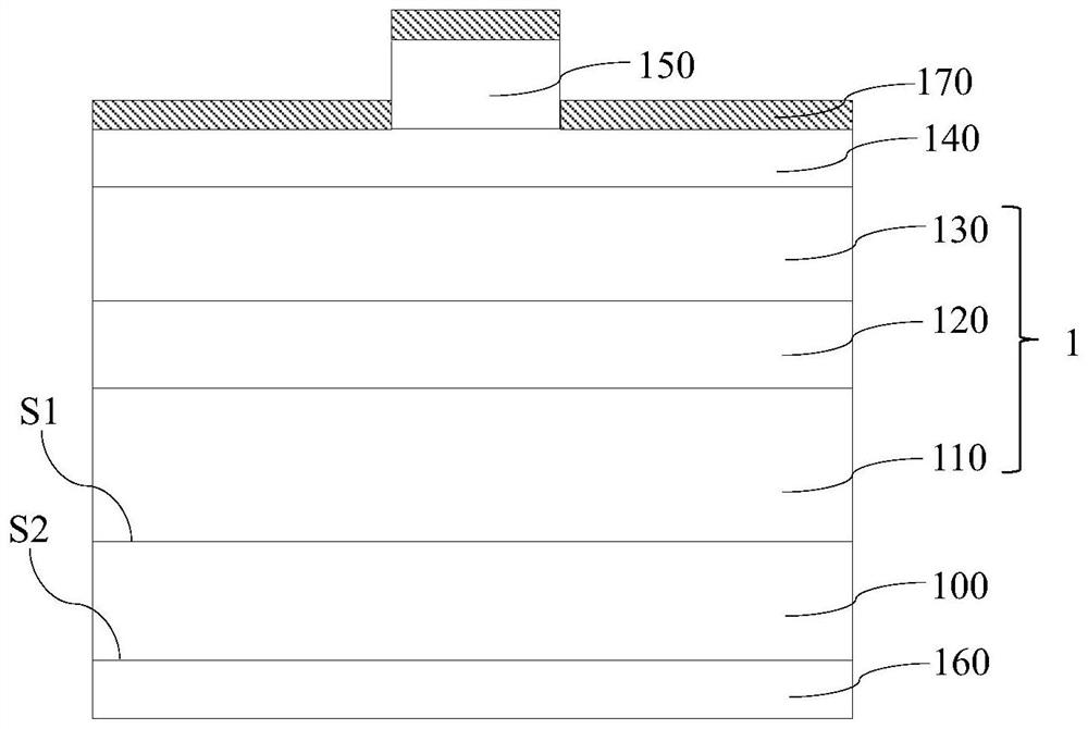
[0053] The present invention provides a light emitting diode as follows, such as Figure 4 The schematic cross-sectional view includes the following stacked layers: 100: substrate; 1: semiconductor epitaxial stack; 110: first conductivity type semiconductor layer; 120: active layer; 130: second conductivity type semiconductor layer; 140: 150: the first electrode; 160: the second electrode; S1: the first surface of the substrate; S2: the second surface of the substrate; 190: an etching stopper layer.
[0054] The details of each structural stack layer are described below.
[0055] The substrate 100 is used for epitaxial growth. In this embodiment, a commonly used GaAs substrate is preferred. It should be noted that the substrate 100 is not limited to GaAs, and other materials such as GaP and InP may also be used.
[0056] In the present embodiment, a commercially available single crystal substrate manufactured by a known manufacturing method can be used as the GaAs substrate 1...
Embodiment 2
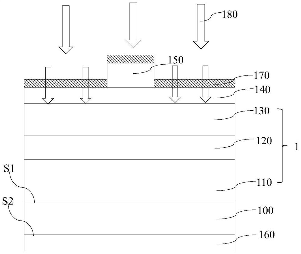
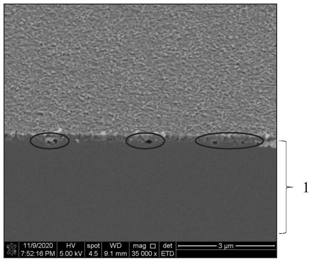
[0076] In order to improve the lattice quality of the semiconductor epitaxial stack 1 and the etching barrier layer 190, reduce the lattice mismatch between the semiconductor epitaxial stack 1 and the etching barrier layer 190, in the semiconductor epitaxial stack 1 and the etching barrier layer 190 Add an intermediate layer 200 between them, such as Figure 5 As shown, the lattice constant of the intermediate layer 200 is between those of the semiconductor epitaxial stack 1 and the etching stopper layer 190 .
[0077] In some embodiments, the material of the intermediate layer 200 is preferably GaInP, and the thickness of the intermediate layer is in the range of 20-50 nm. By adding the intermediate layer 200, the lattice mismatch between the semiconductor epitaxial stack 1 and the etching barrier layer 190 can be reduced, the crystal quality of the etching barrier layer can be improved, and the luminous efficiency of the light emitting diode can be improved.
Embodiment 3
[0079] The manufacturing process of the light emitting diode of the above-mentioned embodiment 2 will be described in detail below.
[0080] First, if Figure 6 As shown, a substrate 100 is provided, and the substrate 100 has a first surface S1 and a second surface S2 opposite to each other; preferably, the substrate 100 is a GaAs substrate; on the first surface S1 of the substrate 100 The first conductivity type semiconductor layer 110 , the active layer 120 and the second conductivity type semiconductor layer 130 are sequentially formed. Specifically, a semiconductor epitaxial stack can be grown sequentially by using MOCVD (metal organic compound chemical vapor deposition) process. Optionally, the semiconductor epitaxial stack includes an N-type layer, a quantum well layer, and a P-type layer in sequence; optionally, the N-type layer includes an N-type buffer layer and an N-type confinement layer in sequence; in this embodiment, the N-type The buffer layer is a GaAs buffer ...
PUM
| Property | Measurement | Unit |
|---|---|---|
| thickness | aaaaa | aaaaa |
| thickness | aaaaa | aaaaa |
| thickness | aaaaa | aaaaa |
Abstract
Description
Claims
Application Information
 - R&D Engineer
- R&D Manager
- IP Professional
- Industry Leading Data Capabilities
- Powerful AI technology
- Patent DNA Extraction
Browse by: Latest US Patents, China's latest patents, Technical Efficacy Thesaurus, Application Domain, Technology Topic, Popular Technical Reports.
© 2024 PatSnap. All rights reserved.Legal|Privacy policy|Modern Slavery Act Transparency Statement|Sitemap|About US| Contact US: help@patsnap.com