Manufacturing method of silicon pressure sensor chip of beam film structure

A technology of sensor chip and manufacturing method, which is applied to the measurement of the property and force of piezoelectric resistance materials, etc., can solve the problems of depth error and difficulty in obtaining beam film thickness, etc., and achieve improved consistency, simple operation, and clear production process Effect

Active Publication Date: 2021-12-14
EAST CHINA INST OF OPTOELECTRONICS INTEGRATEDDEVICE
View PDF10 Cites 0 Cited by
  • Summary
  • Abstract
  • Description
  • Claims
  • Application Information

AI Technical Summary

Problems solved by technology

The problem with this method is that there will be a certain depth error in the front etching or etching, and it is difficult to obtain an accurate thickness of the beam film thickness in the actual process.

Method used


Image

  • Manufacturing method of silicon pressure sensor chip of beam film structure
  • Manufacturing method of silicon pressure sensor chip of beam film structure
  • Manufacturing method of silicon pressure sensor chip of beam film structure

Examples


Embodiment Construction

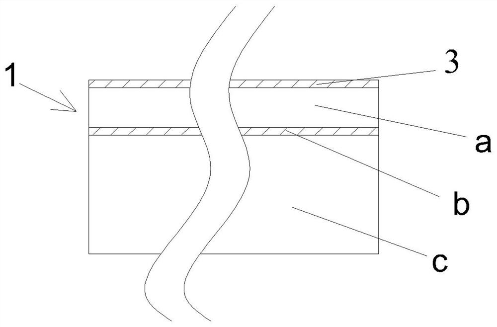
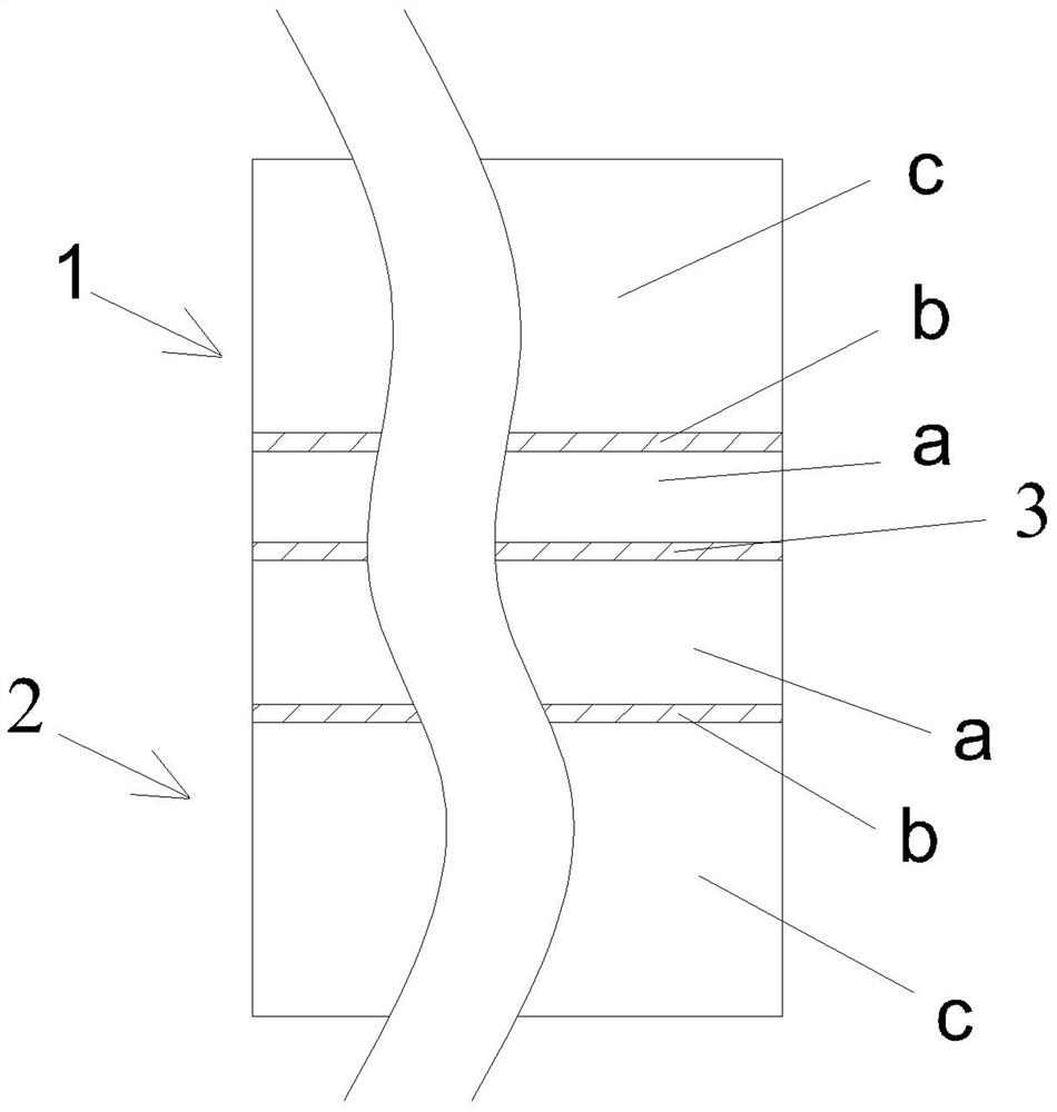
[0028] like Figure 1-9 As shown, a silicon pressure sensor chip manufacturing method with a beam-membrane structure includes the following steps: a) bonding the first silicon wafer and the second silicon wafer, and selecting two SOI silicon wafers as the first silicon wafer 1 and the second silicon wafer The second silicon wafer 2, the first and second silicon wafers have the same structure and both include a top layer of silicon a, a buried oxide layer b and a bottom layer of silicon c. On the top layer of silicon a of the first silicon wafer, an oxide layer 3 is prepared by performing a thermal oxidation process, and the oxide layer 3 and the top layer of silicon a of the second silicon wafer 2 are used as bonding surfaces to perform silicon-silicon dioxide bonding. Bonding, that is, bonding the second silicon chip 2 to the oxide layer 3 of the first silicon chip.

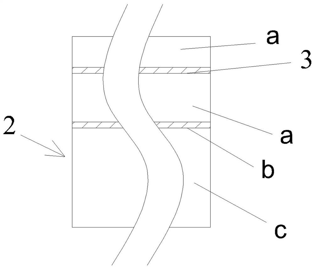
[0029] b) Thinning of the first silicon wafer, the buried oxide layer b and the underlying silicon c of the ...


PUM


Abstract

The invention provides a manufacturing method of a silicon pressure sensor chip of a beam film structure. The manufacturing method comprises the following steps of a) bonding of a first silicon wafer and a second silicon wafer, b) thinning of the first silicon wafer, c) manufacturing of a piezoresistor, d) manufacturing of a piezoresistor bridge, e) manufacturing of a beam structure and f) manufacturing of a back cavity. The method is simple and practical to operate and clear in manufacturing process, the thickness of the silicon beam and the thickness of the silicon film can be accurately controlled, and the consistency of the performance of the pressure sensor chip is improved.

Description

Technical field: The invention relates to the field of silicon pressure sensor chip manufacturing, in particular to a method for manufacturing a silicon pressure sensor chip with a beam-membrane structure. Background technique: MEMS silicon pressure sensor is the most important type of sensor in current life and production, and is widely used in the fields of automobile industry, aerospace industry, military, medical and health care, etc. [0003] The piezoresistive pressure sensor is currently the most widely used type of pressure sensor. Using the good mechanical and electrical properties of silicon, the force-sensitive resistor is implanted into the sensitive film by diffusion or ion implantation to realize the pressure-sensitive element and conversion. Integration of circuits. [0004] The silicon piezoresistive pressure sensor with beam-membrane structure has the advantages of good stress concentration effect, high linearity, and small size, and is a structure commonly...

Claims


Application Information

Patent Timeline
Patent Type & Authority Applications(China)
IPC IPC(8): G01L1/18
CPCG01L1/18Y02P70/50
Inventor 王帆郭立建赵娟喻磊
Owner EAST CHINA INST OF OPTOELECTRONICS INTEGRATEDDEVICE
Why Eureka
Try Eureka