Vertical GaN Schottky diode based on in-situ growth MIS structure and preparation method thereof
A Schottky diode, MIS structure technology, applied in semiconductor/solid-state device manufacturing, semiconductor devices, electrical components, etc., can solve problems such as poor interface quality and affect device characteristics, achieve high interface quality, inhibit reverse leakage, The effect of less interface state
- Summary
- Abstract
- Description
- Claims
- Application Information
AI Technical Summary
Problems solved by technology
Method used
Image
Examples
preparation example Construction
[0033] like figure 2 As shown, the present invention also provides a method for preparing the above-mentioned vertical GaN Schottky diode based on the in-situ growth MIS structure, which specifically includes the following steps:
[0034] S1. Provide a substrate, ultrasonically clean the substrate 1 with acetone, absolute ethanol solution, and deionized water, and heat-treat the substrate 1 at 1050°C for 10 minutes in a hydrogen atmosphere, and then use metal organic compound chemical vapor deposition An n+ layer 2 with a thickness of 0.5-5 μm is deposited on the substrate 1 by MOCVD process, and the doping concentration is 10 18 cm -3 ~10 20 cm -3 , the doping element is silicon, wherein the reaction chamber pressure in the MOCVD process is 10-100 Torr, the Ga source flow rate is 50-100 μmol / min, the ammonia gas flow rate is 3000-6000 sccm, the hydrogen gas flow rate is 1000-2000 sccm, and the temperature is 900 °C ;
[0035] S2. On the n+ layer 2, deposit a drift regio...
Embodiment 1
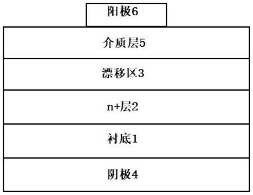
[0040]The vertical GaN Schottky diode based on the in-situ growth MIS structure provided by the embodiment of the present invention includes a substrate 1, the bottom of the substrate 1 is provided with a cathode 4, and the top of the substrate 1 is provided with an n+ layer sequentially from bottom to top 2 and the drift region 3, the top of the drift region 3 is provided with an in-situ grown dielectric layer 5, and the top of the dielectric layer 5 is provided with an anode 6.
[0041] Materials of substrate 1 , n+ layer 2 and drift region 3 are gallium nitride materials, substrate 1 is an n-type GaN substrate, and dielectric layer 5 is made of aluminum nitride.
[0042] The n+ layer 2 has a thickness of 0.5 μm and a doping concentration of 10 18 cm -3 .
[0043] The thicknesses of the drift region 3 and the dielectric layer 5 are 1 μm and 5 nm, respectively.
[0044] Cathode 4 metal adopts Ti / Al / Ni / Au combination, wherein the thickness of Ti metal is 20nm, the thickness...
Embodiment 2
[0053] The vertical GaN Schottky diode based on the in-situ growth MIS structure provided by the embodiment of the present invention includes a substrate 1, the bottom of the substrate 1 is provided with a cathode 4, and the top of the substrate 1 is provided with an n+ layer sequentially from bottom to top 2 and the drift region 3, the top of the drift region 3 is provided with an in-situ grown dielectric layer 5, and the top of the dielectric layer 5 is provided with an anode 6.
[0054] Materials of substrate 1 , n+ layer 2 and drift region 3 are gallium nitride materials, substrate 1 is an n-type GaN substrate, and dielectric layer 5 is made of aluminum nitride.
[0055] The n+ layer 2 has a thickness of 3 μm and a doping concentration of 10 19 cm -3 .
[0056] The thicknesses of the drift region 3 and the dielectric layer 5 are 5 μm and 10 nm, respectively.
[0057] Cathode 4 metal adopts Ti / Al / Ni / Au combination, wherein the thickness of Ti metal is 50nm, the thickness...
PUM
| Property | Measurement | Unit |
|---|---|---|
| thickness | aaaaa | aaaaa |
| thickness | aaaaa | aaaaa |
| thickness | aaaaa | aaaaa |
Abstract
Description
Claims
Application Information
 - R&D Engineer
- R&D Manager
- IP Professional
- Industry Leading Data Capabilities
- Powerful AI technology
- Patent DNA Extraction
Browse by: Latest US Patents, China's latest patents, Technical Efficacy Thesaurus, Application Domain, Technology Topic, Popular Technical Reports.
© 2024 PatSnap. All rights reserved.Legal|Privacy policy|Modern Slavery Act Transparency Statement|Sitemap|About US| Contact US: help@patsnap.com


