Silicon carbide Schottky diode and preparation method thereof
A technology of Schottky diodes and silicon carbide, which is applied in semiconductor/solid-state device manufacturing, semiconductor devices, electrical components, etc., can solve the problems of increased Schottky reverse leakage and large reverse leakage of SiCJBS to improve performance Effect
- Summary
- Abstract
- Description
- Claims
- Application Information
AI Technical Summary
Problems solved by technology
Method used
Image
Examples
Embodiment 1
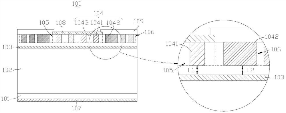
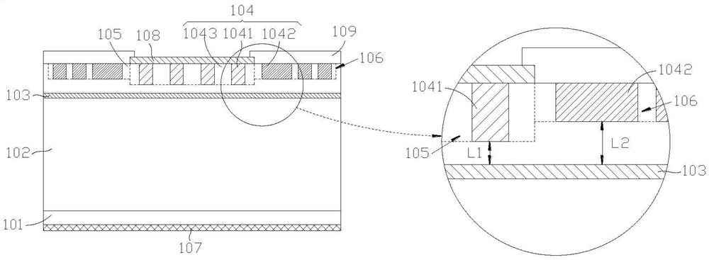
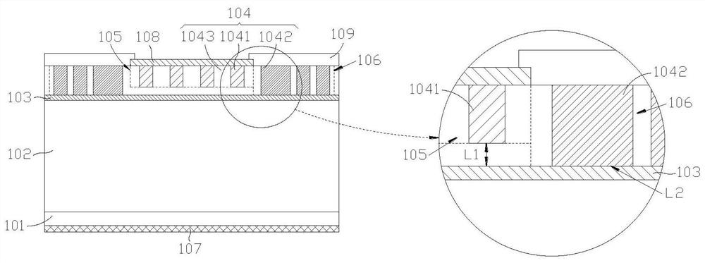
[0053] Such as Figure 1a As shown, in order to solve the problem of excessive reverse leakage of SiC JBS, especially when the reverse bias voltage is low, the Schottky reverse leakage increases rapidly with the increase of voltage, some embodiments of the present disclosure provide a A silicon carbide Schottky diode 100 includes: a SiC substrate 101 , a drift layer 102 , a barrier layer 103 , a transition layer 104 , a cathode 107 , an anode 108 and a protection layer 109 .
[0054] Exemplarily, the SiC substrate 101 is a SiC substrate of the first conductivity type, and the thickness of the SiC substrate 101 is 350 um to 500 um.
[0055] The drift layer 102 is a drift layer of the first conductivity type, located above the SiC substrate 101 , and the thickness of the drift layer 102 formed by epitaxy is 5 um to 150 um according to the different withstand voltage capability of the SiC JBS.
[0056] The barrier layer 103 is a barrier layer of the second conductivity type, loca...
Embodiment 2
[0066] The present disclosure also provides a method for preparing a silicon carbide Schottky diode, which is to prepare the silicon carbide Schottky diode in Embodiment 1.
[0067] figure 2 It is a schematic flowchart of a method for preparing a silicon carbide Schottky diode shown in an embodiment of the present disclosure. Figure 3-Figure 9 It is a schematic cross-sectional structure formed by related steps of a method for manufacturing a silicon carbide Schottky diode shown in an embodiment of the present disclosure. Below, refer to figure 2 and Figure 3-Figure 9 The detailed steps of an exemplary method of manufacturing a silicon carbide Schottky diode proposed in an embodiment of the present disclosure will be described.
[0068] Such as figure 2 As shown, the silicon carbide Schottky diode preparation method of this embodiment includes the following steps:
[0069] Step S101 : providing a first conductivity type SiC substrate 101 .
[0070] Wherein, the wafer...
Embodiment 3
[0094] On the basis of Embodiment 2, this embodiment provides a method for preparing an N-type silicon carbide Schottky diode, such as figure 2 As shown, the N-type silicon carbide Schottky diode preparation method of the present embodiment includes the following steps:
[0095] Step S101 : providing an N-type SiC substrate 101 .
[0096] Wherein, the wafer thickness of the SiC substrate 101 is 350um to 500um.
[0097] Step S102: if image 3 , forming an N-type drift layer 102 on the N-type SiC substrate 101 .
[0098] Specifically, the N-type drift layer 102 is formed by CVD epitaxy. The N-type drift layer 102 is a uniformly doped SiC layer. Depending on the withstand voltage capability of the SiC JBS, the thickness of the N-type drift layer 102 formed by epitaxy is 5um to 150um. The doping concentration of N-type ions in the N-type drift layer 102 is 1E14cm -3 to 1E17cm -3 ; During the epitaxy process, the temperature of the cavity is 1400°C to 1800°C.
[0099] Step S...
PUM
| Property | Measurement | Unit |
|---|---|---|
| Thickness | aaaaa | aaaaa |
| Doping concentration | aaaaa | aaaaa |
Abstract
Description
Claims
Application Information
 - R&D Engineer
- R&D Manager
- IP Professional
- Industry Leading Data Capabilities
- Powerful AI technology
- Patent DNA Extraction
Browse by: Latest US Patents, China's latest patents, Technical Efficacy Thesaurus, Application Domain, Technology Topic, Popular Technical Reports.
© 2024 PatSnap. All rights reserved.Legal|Privacy policy|Modern Slavery Act Transparency Statement|Sitemap|About US| Contact US: help@patsnap.com


