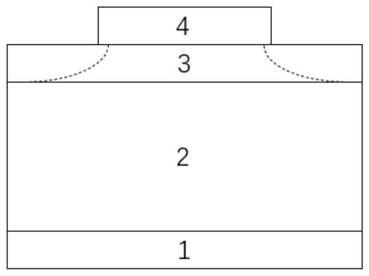
Vertical aluminum nitride schottky diode based on silicon carbide substrate and its preparation method
A Schottky diode and silicon carbide substrate technology, which is applied in the field of Schottky aluminum nitride diodes, can solve the problems of low breakdown voltage, undeveloped aluminum nitride, and low rated power, so as to improve the breakdown voltage , Inhibit reverse leakage and improve quality
- Summary
- Abstract
- Description
- Claims
- Application Information
AI Technical Summary
Problems solved by technology
Method used
Image
Examples
Embodiment 1
[0026] Example 1, making an aluminum nitride Schottky diode with Ni / Au as the anode metal, titanium as the cathode metal, and magnesium ions as the ion implantation.
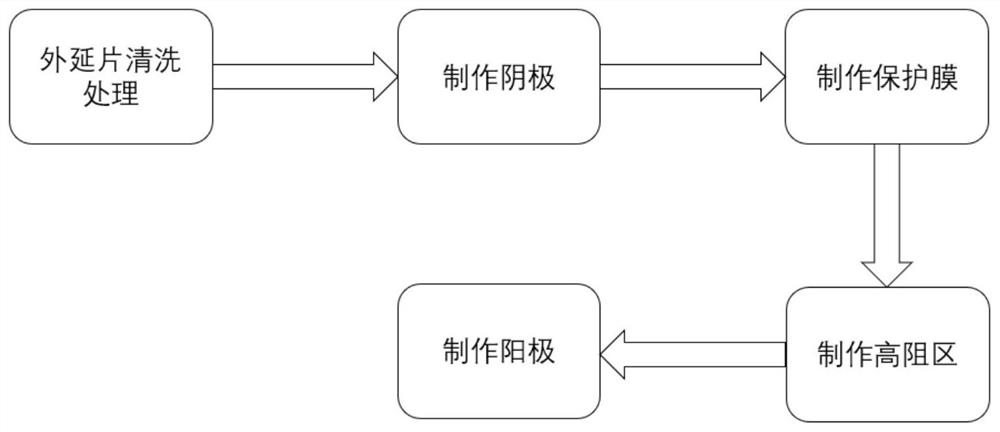
[0027] Step 1: Cleaning the epitaxial wafer.
[0028] 1.1) Selection of epitaxial wafers:
[0029] The epitaxial wafer used in this embodiment includes an n-type highly doped silicon carbide substrate and an epitaxial wafer material of an n-type aluminum nitride epitaxial layer from bottom to top, wherein the thickness of the silicon carbide substrate is 400 μm, and the doping concentration is 5×10 18 cm -3 , the thickness of the n-type aluminum nitride epitaxial layer is 500nm, and the doping concentration is 1×10 17 cm -3 .
[0030] 1.2) Pretreatment of the epitaxial wafer:
[0031] Put the above-mentioned epitaxial wafer into acetone, isopropanol, and deionized water for 5 minutes, and then soak the epitaxial wafer in 10% HF solution for 30 s, and finally wash the epitaxial wafer with deionized water an...
Embodiment 2
[0041] Embodiment 2: Fabricate an aluminum nitride Schottky diode in which the anode metal is Ni / Au / Ni, the cathode metal is nickel, and the ion implantation is nitrogen ions.
[0042] Step A: select the epitaxial wafer and clean it.
[0043] A1) Select epitaxial wafer materials including n-type highly doped silicon carbide substrate and n-type aluminum nitride epitaxial layer from bottom to top, wherein the thickness of the silicon carbide substrate is 100 μm, and the doping concentration is 5×10 17 cm -3 , the thickness of the n-type aluminum nitride epitaxial layer is 800nm, and the doping concentration is 1×1015 cm -3 epitaxial wafers;
[0044] A2) Put the above-mentioned epitaxial wafer into acetone, isopropanol, and deionized water for 5 minutes, and then soak the epitaxial wafer in 10% HF solution for 30 seconds. Finally, wash the epitaxial wafer with deionized water and dry it with nitrogen. .
[0045] Step B: deposit cathode metal on the highly doped n-type silico...
Embodiment 3
[0054] Example 3, making an aluminum nitride Schottky diode in which the anode metal is Pt / Au, the cathode metal is Ti / Al, and the ion implantation is fluorine ions.
[0055] Step 1: Select an epitaxial wafer and clean it.
[0056] The epitaxial wafer material including n-type highly doped silicon carbide substrate and n-type aluminum nitride epitaxial layer is selected from bottom to top, wherein the thickness of the silicon carbide substrate is 5000 μm, and the doping concentration is 1×10 20 cm -3 , the thickness of the n-type AlN epitaxial layer is 20 μm, and the doping concentration is 1×10 17 cm -3 ; then put the epitaxial wafer into acetone, isopropanol, and deionized water for 5 minutes for ultrasonic cleaning; then put the epitaxial wafer into 10% HF solution for 30 seconds; finally wash the epitaxial wafer with deionized water and dry it with nitrogen .
[0057] Step 2: Deposit cathode metal on the highly doped n-type silicon carbide substrate, and anneal the cat...
PUM
| Property | Measurement | Unit |
|---|---|---|
| thickness | aaaaa | aaaaa |
| thickness | aaaaa | aaaaa |
| thickness | aaaaa | aaaaa |
Abstract
Description
Claims
Application Information
 - R&D Engineer
- R&D Manager
- IP Professional
- Industry Leading Data Capabilities
- Powerful AI technology
- Patent DNA Extraction
Browse by: Latest US Patents, China's latest patents, Technical Efficacy Thesaurus, Application Domain, Technology Topic, Popular Technical Reports.
© 2024 PatSnap. All rights reserved.Legal|Privacy policy|Modern Slavery Act Transparency Statement|Sitemap|About US| Contact US: help@patsnap.com


