TSV-based three-dimensional integrated circuit packaging method

A technology of integrated circuits and packaging methods, applied in circuits, electrical components, electrical solid devices, etc., can solve the problems of micro-cracks on the surface of wafers, easy generation of debris, and influence of chip thermo-mechanical reliability.

Pending Publication Date: 2021-09-10
成都优拓优联万江科技有限公司
View PDF6 Cites 0 Cited by
  • Summary
  • Abstract
  • Description
  • Claims
  • Application Information

AI Technical Summary

Problems solved by technology

[0003] 1. When the traditional packaging process planarizes the TSV CMP through-hole copper dish depression and copper protrusion defect, the polishing effect is not good, and debris is easily generated during polishing;
[0004] 2. During the thinning process of ultra-thin wafers, the grinding force generated by the high-speed rotating grinding wheel will cause surface micro-cracks and sub-surface cracks on the wafer surface.
[0006] 3. Since the core structure of TSV is composed of copper and silicon composites with large differences in the number of thermal expansion systems, temperature changes during the manufacturing process will generate thermal mismatch internal stress, which reduces the thermomechanical stability of the TSV package
[0007] For example, the patent application with the application number CN201610040115.2 discloses a wafer-level packaging method for micro-nano electromechanical wafers. A groove is made on the front side of a silicon wafer to protect the micromechanical components on the front side of the MEMS wafer. Make through-silicon holes through the front and back of the silicon wafer, form an insulating layer on the side walls of the through-silicon holes, and obtain a cover plate; make metal pads on the electrodes on the front of the MEMS wafer; connect the front of the cover plate and the The front side bonding of the MEMS wafer, wherein the metal pad corresponds to the position of the through-silicon via, and the metal pad covers at least a part of the through-silicon via; the liquid metal microhole filling technology is used to fill the through-silicon via Filling, so that the filled liquid metal is bonded to the metal pad. Although this technical solution can realize the electrical interconnection from the MEMS wafer electrode to the back of the cover plate, this packaging method cannot improve the shear rate of the bonded chipset. cutting strength and will affect the overall thermomechanical reliability of the chip

Method used


Image

  • TSV-based three-dimensional integrated circuit packaging method

Examples


Embodiment Construction

[0032] In order to have a clearer understanding of the technical features, purposes and effects of the present invention, the specific implementation manners of the present invention will now be described with reference to the accompanying drawings.

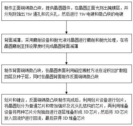
[0033] In this example, if figure 1 As shown, a TSV-based three-dimensional integrated circuit packaging method, the method specifically includes: Step 1: making front copper-tin micro-bumps, providing wafer devices, photoetching a mask layer on the front of the wafer, and etching out TSV through holes and countersunk holes, and then TSV electroplating and electroplating of micro-bumps; Step 2: Backside thinning, grinding and polishing the wafer with grinding equipment and polishing liquid, and grinding the wafer to Thinning of the back of the wafer is completed when the thickness is preset; step 3: making micro-bumps of copper and tin on the back, and depositing a diffusion barrier layer and a seed layer on the surface of the wa...


PUM

PropertyMeasurementUnit
Thicknessaaaaaaaaaa

Abstract

The invention discloses a TSV-based three-dimensional integrated circuit packaging method, which comprises the following steps of: providing a wafer device, photoetching a mask layer on the front surface of the wafer, respectively etching a TSV through hole and a counterbore, and then carrying out TSV electroplating and micro bump electroplating, grinding and polishing the wafer by adopting grinding equipment and a polishing solution, and grinding the wafer to a preset thickness, depositing a diffusion barrier layer and a seed layer on the surface of the wafer by using a magnetron sputtering method, and manufacturing a reverse copper-tin micro bump on the reverse side of the wafer, and scribing by using scribing equipment to divide the wafer into a common chip and a chip with a reinforcing ring and a counterbore structure, independently stacking the two kinds of chips layer by layer by using stacking equipment to form 3D chips, putting the 3D chips into a reflux oven, and refluxing to finally obtain the 3D stacked chip. According to the invention, the key packaging technology of the integrated circuit is optimized, the damage and residual stress generated by wafer grinding are reduced, and the thermal mechanical stability and polishing effect of the TSV packaging body are improved.

Description

technical field [0001] The invention relates to the field of integrated circuit packaging, in particular to a TSV-based three-dimensional integrated circuit packaging method. Background technique [0002] Integrated circuit packaging not only plays the role of electrical connection between the bonding point of the integrated circuit chip and the outside, but also provides a stable and reliable working environment for the integrated circuit chip, and plays a role in mechanical or environmental protection for the integrated circuit chip, so that the integrated circuit The chip can perform normal functions, and its high stability and reliability are guaranteed. In short, the quality of integrated circuit packaging has a great relationship with the overall performance of integrated circuits. The existing problems of integrated circuit packaging technology are as follows: [0003] 1. When the traditional packaging process planarizes the TSV CMP through-hole copper dish depressi...

Claims


Application Information

Patent Timeline
IPC IPC(8): H01L21/60H01L21/768H01L25/18H01L21/306
CPCH01L21/76898H01L24/03H01L24/11H01L24/81H01L24/82H01L25/18H01L21/30625H01L2224/82951
Inventor 何兵李峰
Owner 成都优拓优联万江科技有限公司
Why Eureka
Try Eureka