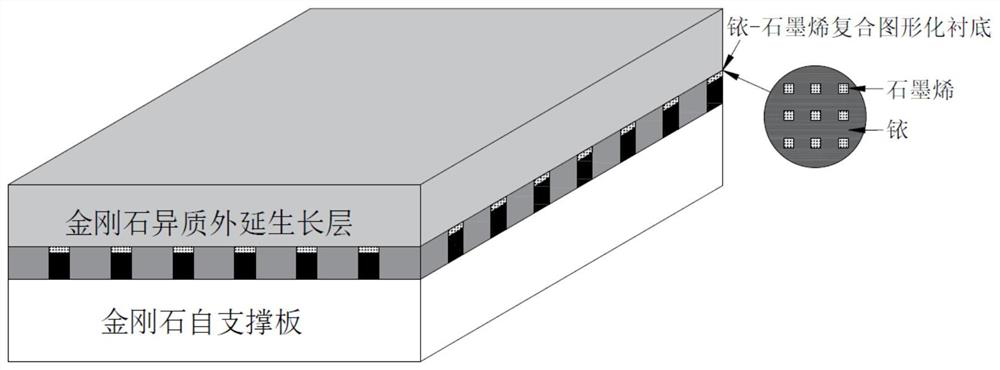
Epitaxial Growth Method of Single Crystal Diamond Based on Iridium-Graphene Structured Buffer Layer
A single crystal diamond, epitaxial growth technology, applied in the direction of single crystal growth, single crystal growth, crystal growth, etc., can solve the problems of thermal expansion mismatch, low single crystal, lattice mismatch, etc., to achieve low stress and low quality. Effect
- Summary
- Abstract
- Description
- Claims
- Application Information
AI Technical Summary
Problems solved by technology
Method used
Image
Examples
Embodiment 1
[0030] (1) The diamond self-supporting plate has been precision ground and polished to a surface roughness of less than 0.5nm, and it is subjected to pickling pretreatment; (2) Spin-coating photoresist on the diamond, and using photolithography to prepare a set Patterned area, the area of this area accounts for 50% of the total area, and then use the magnetron sputtering method to deposit a metal iridium film to 100nm at a rate of 2nm / min at a temperature of 600°C, and then deposit the photoresist film and the Iridium film peeling; spin-coat photoresist on the patterned iridium / diamond laminated substrate, use photolithography to prepare a photoresist area covering the iridium layer, and use magnetron sputtering on the surface at 200 ° C With the speed deposition of 5nm / min and the thick metallic nickel film of iridium layer; (3) then carry out 10min vacuum annealing to it with 600 ℃; (4) then control the ratio of methane and hydrogen in the process of microwave plasma chemic...
Embodiment 2
[0032] (1) The diamond self-supporting plate has been precision ground and polished to a surface roughness of less than 0.5nm, and it is subjected to pickling pretreatment; (2) Spin-coating photoresist on the diamond, and using photolithography to prepare a set Patterned area, the area of this area accounts for 50% of the total area, and then utilizes the magnetron sputtering method to deposit a metal iridium film to 200nm at a speed of 4nm / min at a temperature of 800°C, and then deposit the photoresist film and the iridium on it Film peeling; Spin-coat photoresist on the patterned iridium / diamond laminated substrate, use photolithography to prepare a photoresist area covering the iridium layer, and use magnetron sputtering method on the surface at 300 ° C to 10nm / min speed deposition and iridium layer equal thickness metal nickel film; (3) followed by vacuum annealing at 600°C for 20min; (4) followed by controlling the ratio of methane to hydrogen in the process of microwave...
Embodiment 3
[0034](1) The diamond self-supporting plate has been precision ground and polished to a surface roughness of less than 0.5nm, and it is subjected to pickling pretreatment; (2) Spin-coating photoresist on the diamond, and using photolithography to prepare a set Patterned area, the area of this area accounts for 60% of the total area, then use the magnetron sputtering method to deposit a metal iridium film to 400nm at a speed of 6nm / min at a temperature of 800°C, and then deposit the photoresist film and the Iridium film peeling; Spin-coat photoresist on the patterned iridium / diamond laminated substrate, use photolithography to prepare the photoresist area covering the iridium layer, and use magnetron sputtering method on the surface at 400 ° C With the speed deposition of 15nm / min and the thick metallic nickel film of iridium layer; (3) then carry out 30min vacuum annealing to it with 800 ℃; (4) the ratio of methane and hydrogen in the microwave plasma chemical vapor depositio...
PUM
| Property | Measurement | Unit |
|---|---|---|
| surface roughness | aaaaa | aaaaa |
Abstract
Description
Claims
Application Information
 - R&D Engineer
- R&D Manager
- IP Professional
- Industry Leading Data Capabilities
- Powerful AI technology
- Patent DNA Extraction
Browse by: Latest US Patents, China's latest patents, Technical Efficacy Thesaurus, Application Domain, Technology Topic, Popular Technical Reports.
© 2024 PatSnap. All rights reserved.Legal|Privacy policy|Modern Slavery Act Transparency Statement|Sitemap|About US| Contact US: help@patsnap.com


