High-temperature-resistant electrode with doped oxide metal gradient layer and preparation method of high-temperature-resistant electrode
A technology of oxide and gradient layer, which is applied in metal material coating process, superimposed layer plating, piezoelectric/electrostrictive device manufacturing/assembly, etc., can solve the problem that the degradation temperature cannot reach 1000°C, and achieve Improve degradation, improve high-temperature conductivity, and have remarkable effects in high-temperature resistance
- Summary
- Abstract
- Description
- Claims
- Application Information
AI Technical Summary
Problems solved by technology
Method used
Image
Examples
Embodiment 1
[0046] Step 1, the substrate is sequentially washed with acetone, alcohol and deionized water, and remove organic pollutants on the surface, and then blow dry with nitrogen.
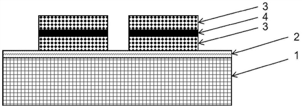
[0047] Step 2, the substrate after steps will be placed in an atomic layer deposition system (the model is ALD150LX of the US Kurtj.lesker), and the vacuum, deposited 20 nm high temperature oxide layer.
[0048] Step three, apply a photoresist (Model AR-P5350) on the high temperature oxide layer, complete the hierarchy and bake with the uniformity-hot plate all-in-one (model of the American CEE's Apo II). The photolithography (model is MA6 / BA6 of Germany Karlsuss), forms a mask, placed in a mixture of developers (Model AR300-26) and water in a mixture of 1: 7 ratio, last used Ion washing washed with a development to obtain a doped oxide metal gradient layer pattern.
[0049] Step 4, the sample after step three-shot is placed on the substrate table of the magnetron sputtering system (model of DISCOVERY635, ...
Embodiment 2
[0054] Based on the first embodiment, in step four, the metal target is a PT target, and the oxide target is Al. 2 O 3 Target.
[0055] Example 2 had a high temperature resistant electrode having a doped oxide metal gradient layer, tested, maintained at 1200 ° C, still maintaining a good surface morphology, such as Figure 4 As shown, although there are some tiny holes, it does not affect the continuity of the electrode. It can be seen that the electrode structure of the present invention, high temperature resistance, has good application prospects.
Embodiment 3
[0057] Step 1, the substrate is sequentially washed with acetone, alcohol and deionized water, and remove organic pollutants on the surface, and then blow dry with nitrogen.
[0058] Step 2, the substrate after the step is placed in an atomic layer deposition system, vacuum, deposited 20 nm high temperature oxide layer.
[0059] Step three, apply a photoresist on the high temperature oxide layer, complete the hierarchy with the baking with a split-hot plate, and then use the photolithography, form a mask, and add the developer and water to press 1. : 7 ratio of 22S in a mixed mixture, and finally washed with deionized water to obtain a doped oxide metal gradation layer pattern.
[0060] Step 4, the sample after step three-shot is placed on the substrate table of the magnetron sputtering system (model of DISCOVERY635, US Denton, and then put the substrate stage into the vacuum chamber, carrying a metal target Common sputtering with the oxide target, a 100 nm thick oxide metal gradi...
PUM
 Abstract
Description
Claims
Application Information
 - R&D
- Intellectual Property
- Life Sciences
- Materials
- Tech Scout
- Unparalleled Data Quality
- Higher Quality Content
- 60% Fewer Hallucinations
Browse by: Latest US Patents, China's latest patents, Technical Efficacy Thesaurus, Application Domain, Technology Topic, Popular Technical Reports.
© 2025 PatSnap. All rights reserved.Legal|Privacy policy|Modern Slavery Act Transparency Statement|Sitemap|About US| Contact US: help@patsnap.com


