Method for manufacturing two-stage micro-nano structure array based on template
A micro-nano structure and array technology, applied in the manufacture of micro-structure devices, micro-structure technology, micro-structure devices, etc., can solve problems such as poor bonding strength, alignment, and nano-film shedding, and achieve good strength, long life, and high efficiency Effect
- Summary
- Abstract
- Description
- Claims
- Application Information
AI Technical Summary
Problems solved by technology
Method used
Image
Examples
Embodiment 1
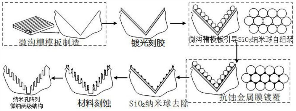
[0037] like figure 1 As shown, this embodiment provides a method for manufacturing a two-level micro-nano structure array based on a template, including the following steps:
[0038] Step 1, micro-groove template manufacturing, using diamond tool ultra-precision cutting technology to process high-quality micro-groove arrays on the surface of workpieces (copper, aluminum, resin, nickel phosphide, etc.) (micro-groove period d = 1 ~ 100 μm) , the parallelism of the micro-groove array should be kept within 1% (parallelism deviation to period ratio), and the surface roughness of the micro-groove should be less than 10nm to ensure that the subsequent SiO 2 The orderliness of nanosphere self-assembly.
[0039] Step 2, first coat a layer of uniform photoresist (such as SU-8, PMMA, PDMS, PS, etc.) on the high-quality micro-groove template and cure the photoresist on the surface of the micro-groove by drying or ultraviolet radiation, The photoresist thickness is controlled within 1 μm...
Embodiment 2
[0047] This embodiment is an improvement on the basis of the first embodiment, and its improvement lies in: figure 2 As shown, in the seventh step, the material etching includes a first angle etching and a second angle etching.
[0048] Specifically, in the first angle etching, the thin-layer mesh-shaped resist metal layer is used as the masking film, and the dry etching (ICP) method is used to selectively select the direction parallel to the second etching surface 2 of the micro-trench template. Remove the circular photoresist and workpiece areas that are not covered by the masking film on the first etching surface 1, the circular area has the same diameter as the self-assembled nanosphere, and the direction of the nanohole is parallel to the second etching face 2 direction.
[0049] In the second angle etching, the thin mesh-shaped resist metal layer is used as the mask film, and the dry etching (ICP) method is used to selectively etch the second The circular photoresist ...
PUM
| Property | Measurement | Unit |
|---|---|---|
| diameter | aaaaa | aaaaa |
| thickness | aaaaa | aaaaa |
| thickness | aaaaa | aaaaa |
Abstract
Description
Claims
Application Information
 - R&D
- Intellectual Property
- Life Sciences
- Materials
- Tech Scout
- Unparalleled Data Quality
- Higher Quality Content
- 60% Fewer Hallucinations
Browse by: Latest US Patents, China's latest patents, Technical Efficacy Thesaurus, Application Domain, Technology Topic, Popular Technical Reports.
© 2025 PatSnap. All rights reserved.Legal|Privacy policy|Modern Slavery Act Transparency Statement|Sitemap|About US| Contact US: help@patsnap.com


